International Journal of Advanced Research in Electrical, Electronics and Instrumentation Engineering
ISSN ONLINE(2278-8875) PRINT (2320-3765)
ISSN ONLINE(2278-8875) PRINT (2320-3765)
| Miteshwar Patel PG Student [VLSI & Embedded Systems], Dept. of EC, U. V. Patel College of Engineering, Ganpat University, Kherva, Mehsana, Gujarat, India |
| Related article at Pubmed, Scholar Google |
Visit for more related articles at International Journal of Advanced Research in Electrical, Electronics and Instrumentation Engineering
Project paper discussing Design For Testability flow of a given ASIC design. As the technology trends to continuously shrink from small scale integration (SSI) to very large scale integration (VLSI), design for testability is also included more seriously into the ASIC flow. This paper describes what, why and how Design-For-Testability done. Scan insertion is performed on RTL to convert design into scan design. Automatic Test Pattern Generation is done for scan inserted design considering test power and its reduction. And at last pattern validation is performed before it is passed to ATE to detect real defects in the design.
Keywords |
||||||||||||
| Automatic test pattern generation, Design for testability, Pattern Validation, Power aware ATPG, scan insertion, Standard Test Interface Language. | ||||||||||||
INTRODUCTION |
||||||||||||
| The semiconductor industry has evolved from the first IC's of the early 1960s and matured rapidly since then. Early small-scale integration (SSI) IC's contained a few (1 to 10) logic gates, amounting to a few tens of transistors. The era of medium-scale integration (MSI) increased the range of integrated logic available to counters and similar, larger scale, logic functions. The era of large-scale integration (LSI) packed even larger logic functions, such as the first microprocessors, into a single chip. The era of very large-scale integration (VLSI) now offers 64-bit microprocessors, complete with cache memory and floating-point arithmetic units, well over a million transistors on a single piece of silicon. As CMOS process technology improves, transistors continue to get smaller and IC's hold more and more transistors. Some people use the term ultra-large scale integration (ULSI), but most people stop at the term VLSI. | ||||||||||||
| With Increase in complex system, testability is an increasing concern in almost every application and in every area of application development. Test engineers put more efforts in addressing the issue of testability at the device, board, and system levels deliver more consistently reliable and cost effective products to the market place. This means building an test capabilities in every phase of development and deployment, including design verification, hardware and software integration, manufacturing, and in the field. | ||||||||||||
| The sooner the process and electrical defects are caught, the lower the total cost of ownership will be. Defect finding and analysis at early manufacturing stages are critical to lower cycle time and cost for high volume production. Therefore, key challenge facing manufactures of high complexity system on chips is the issue of test strategies. Designfor- testability is a key to lower life cycle cost of the product from the design, manufacturing and the field support. In order to improve test quality, a special attention should be given to design to testability at early design stages while defining test process strategy for high volume production. The tests generally are driven by test program that execute in Automatic Test Equipment (ATE) or, in the case of system maintenance, inside the assembled system itself. In addition to finding and indicating the presence of defect, test may be able to log diagnostic information about the nature of the encountered test fails. This diagnostic information can be used to locate the source of the failure. | ||||||||||||
| Failures in integrated circuits can be characterized according to their duration, permanent or temporary, and by their mode, parameter degradation or incorrect design. Figure 1 shows classifications of IC failures. | ||||||||||||
| To protect IC from above mentioned failures, Design for Testability is introduced in VLSI flow. All the failures are detected after fabrication to reduce yield and rejection ratio of IC fabrication. | ||||||||||||
| Design-For-Testability is considered at various stages in ASIC flow shown in Figure 2. Design is converted into scan inserted design which will be in parallel with synthesis. The scan inserted netlist is provided to ATPG tool for pattern generation. Patterns after validation provided to ATE with definition of testing to catch real defects from silicon of design after fabrication. | ||||||||||||
| This project paper presents briefly about what is DFT, and how it is implemented in section 2. Section 3 discuss scan insertion flow on unmapped design using DFT compiler. Section 4 discuss Automatic Test Pattern Generation flow for pattern to detect real defects at ATE. Section 5 discuss Power aware ATPG to understand test power and methods to reduce them. Section 6 discuss pattern validation flow using VCS and clean patterns with respect to parameters defined for testing. | ||||||||||||
DESIGN FOR TESTABILITY |
||||||||||||
| Design For Test is a name for design techniques that add certain testability features to a microelectronic hardware product design. The premise of the added features is that they make it easier to develop and apply manufacturing test for design hardware. The purpose of manufacturing test is to validate that the product hardware contains no defects that could adversely affect the product's correct functioning. | ||||||||||||
| Testability is the combination of two properties of a design: Controllability and Observability (Objective of DFT). Where controllability reflects the difficulty of setting a signal line to a required logic value from primary inputs and observability reflects the difficulty of propagating the logic value of the signal line to primary outputs. | ||||||||||||
| Design for testability (DFT) refers to those design techniques that make the task of subsequent testing easier. There is definitely no single methodology that solves all embedded system-testing problems. There also is no single DFT technique, which is effective for all kinds of circuits. DFT techniques can largely be divided into two categories, i.e., ad hoc techniques and structured (systematic) techniques. | ||||||||||||
| ? DFT methods for digital circuits: | ||||||||||||
| ? Ad-hoc methods | ||||||||||||
| ? Structured methods: | ||||||||||||
| ? Scan Design | ||||||||||||
| ? Partial Scan Design | ||||||||||||
| ? Built-in self-test | ||||||||||||
| ? Boundary scan | ||||||||||||
| we describe three widely used scan cell designs as: | ||||||||||||
| ? MUXed-D Scan Cell | ||||||||||||
| ? Clocked Scan Cell | ||||||||||||
| ? LSSD Scan Cell | ||||||||||||
| In order to implement scan into a design, the design must comply with a set of scan design rules. In addition, a set of design styles must be avoided, as they may limit the fault coverage that can be achieved. A number of scan design rules that are required to successfully utilize scan and achieve the target fault coverage goal are listed in Table 1. In this table, a possible solution is recommended for each scan design rule violation. Scan design rules that are labeled “avoid” must be fixed throughout the shift and capture operations. Scan design rules that are labeled “avoid during shift” must be fixed only during the shift operation. Detailed descriptions are provided for some critical scan design rules. | ||||||||||||
SCAN INSERTION FLOW |
||||||||||||
| The basic process consists of the following tasks: | ||||||||||||
| ? Synthesizing Your Design | ||||||||||||
| ? Post processing Your Design | ||||||||||||
| ? Building Scan Chains: Scan ready and Scan insertion | ||||||||||||
| ? Exporting a Design to TetraMAX ATPG | ||||||||||||
| Complete scan insertion flow for unmapped design using DFT compiler (synopsys) is shown in Figure 3 [1]. figure shows three phase in scan insertion. | ||||||||||||
| Synthesis consists of conversion from RTL to gate level netlist. Optimization and mapping is done during synthesis process. Applying constraints according to design and compiling the design. Post processing consists of checking the violation of all the constraints applied, cleaning them, if observed and finalize it for scan insertion. | ||||||||||||
| Second phase is building scan chains by providing scan information in terms of scan I/Os, clocks, set/reset, test signals and scan configuration. After the scan ready protocol and design is created, scan insertion is done. | ||||||||||||
| Scan ready compilation is performed, Post DRC are checked and cleaned if observed. Test protocol file containing information of all scan information is generated. After successful scan insertion without pre and post DRC, it is then passed with spf to TetraMAX for ATPG. | ||||||||||||
| At last scan insertion, scan verification is also conducted for scan capture and shift operation. | ||||||||||||
AUTOMATIC TEST PATTERN GENERATION FLOW |
||||||||||||
| The goal of ATPG is to create a set of patterns that achieves a given test coverage, where test coverage is the total percentage of testable faults the patterns set actually defect. The ATPG run itself consist of two main steps i.e. generating patterns and fault simulation to determine which faults the pattern detect. The two most typical methods for pattern generation are random and deterministic. Additionally, the ATPG tool can fault simulate patterns from an external set and place those patterns detecting fault in a test set. | ||||||||||||
| TetraMAX is a high-speed, high-capacity automatic test pattern generation (ATPG) tool. It can generate test patterns that maximize test coverage while using a minimum number of test vectors for a wide variety of design types and design flows. It is well suited for designs of all sizes up to millions of gates. With scan testing, the sequential elements of the device are connected into chains and used as primary inputs and primary outputs for testing purposes. Using | ||||||||||||
| ATPG techniques, you can test a much larger number of internal faults than with functional testing alone[3]. | ||||||||||||
| TetraMAX offers three different ATPG modes: Basic-Scan, Fast-Sequential, and Full-Sequential. TetraMAX supports test pattern generation for five types of fault models: stuck-at faults, IDDQ faults, transition delay faults, path delay faults, and bridging faults. It is also compatible with a wide range of design-for-test tools such as DFT Compiler. The design flow using DFT Compiler and TetraMAX ATPG is recommended for maximum ease of use and quality of results. Figure 4 shows GUI of TetraMAX tool and user interface. | ||||||||||||
| General Automatic Test Pattern Generation flow is shown in Figure 5. Scan inserted netlist, with stil procedure file (SPF) generated from DFT compiler is passed to TetraMAX as inputs. Second step is to build internal database for pattern generation. Specific TetraMAX libraries and netlist are combined and for building module definitions. | ||||||||||||
| BULD process takes place in build mode of TetraMAX. And after completion of successful build process SPF file [4], which contains scan definitions are provided to check DRC. Several rule violations are check during DRC mode like clock, verilog syntax, scan chain, set/reset etc. and must be cleared before pattern generation. | ||||||||||||
| After clean DRC mode it automatically transfer mode to TEST mode. Now at last several efforts as per specification are selected and applied for pattern generation. Selecting fault model and test mode, ATPG process starts. | ||||||||||||
| Patterns are generated and stored in different formats like STIL, WGL, Verilog, VHDL, binary and other foundry formats. | ||||||||||||
| Quick estimation of Test and Fault coverage are done after patterns are generated using saved database and results in terms of reports and summaries. | ||||||||||||
| Three possible quality measures are defined as follows: | ||||||||||||
| Test coverage = detected fault / detectable faults. | ||||||||||||
| Test coverage gives the most meaningful measure of test pattern quality and is the default coverage reported in the fault summary report. Test coverage is defined as the percentage of detected faults out of detectable faults, as follows: | ||||||||||||
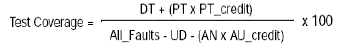 |
||||||||||||
| Fault coverage = detected fault / all faults. | ||||||||||||
| Fault coverage is defined as the percentage of detected faults out of all faults, as follows: | ||||||||||||
| ATPG effectiveness = ATPG resolvable fault / all faults. | ||||||||||||
| ATPG effectiveness is defined as the percentage of ATPG-resolvable faults out of the total faults, as follows: | ||||||||||||
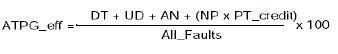 |
||||||||||||
| Report summaries are generated in two forms collapsed and uncollapsed fault summaries. Following results are of stuck – at fault model with basic mode and all desired manual efforts | ||||||||||||
| Uncollapsed Stuck Fault Summary Report | ||||||||||||
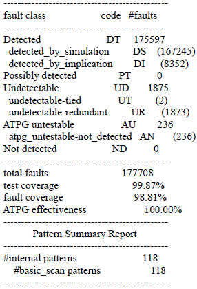 |
||||||||||||
| TetraMAX maintains a list of potential faults in the design and assigns each such fault to a fault class according to its detectability status. Faults classes are organized into categories. A two-character symbol is used as an abbreviated name for both classes and categories. There are five higher-level fault categories containing a total of 11 lower-level fault classes: | ||||||||||||
| DT: detected | ||||||||||||
| DR: detected robustly | ||||||||||||
| DS: detected by simulation | ||||||||||||
| DI: detected by implication | ||||||||||||
| PT: possibly detected | ||||||||||||
| AP: ATPG untestable-possibly detected | ||||||||||||
| NP: not analyzed-possibly detected | ||||||||||||
| UD: undetectable | ||||||||||||
| UU: undetectable unused | ||||||||||||
| UT: undetectable tied | ||||||||||||
| UB: undetectable blocked | ||||||||||||
| UR: undetectable redundant | ||||||||||||
| AU: ATPG untestable | ||||||||||||
| AN: ATPG untestable-not detected | ||||||||||||
| ND: not detected | ||||||||||||
| NC: not controlled | ||||||||||||
| NO: not observed | ||||||||||||
| Results for Stuck – at, iddq and transition fault model are stored in thesis report. | ||||||||||||
POWER AWARE ATPG |
||||||||||||
| Basic ATPG test power reduction techniques are classified into two parts: 1) Shift power Reduction, and 2) Capture power reduction. Following are methods used during ATPG to reduce shift and capture power of design by generating such patterns: | ||||||||||||
| ? Heuristics filling | ||||||||||||
| ? (0 – fill, 1 – fill, MT – fill) | ||||||||||||
| ? Low power test compaction techniques | ||||||||||||
| ? Test Generation (internal constraints checking, external constraints checking, target fault restriction) | ||||||||||||
| MT-filling results in the fewest number of transitions in the scan chains which generally corresponds to the lowest switching activity in the overall circuit, and is thus the preferred approach [5 - 11]. Consider the test cube <1XXX0XX1XX0XX>. By applying the above three non-random filling heuristics, the resulting patterns become: | ||||||||||||
| ? 1111000111000 with MT-filling heuristics | ||||||||||||
| ? 1000000100000 with 0-filling heuristics | ||||||||||||
| ? 1111011111011 with 1-filling heuristics | ||||||||||||
| This above mentioned Heuristic filling methods are applied in the project, and result of power-aware ATPG, approximately 20% average shift power and 10% peak shift power is reduced for stuck-at fault model, also 10% average capture power and 20% peak capture power is reduced for transition fault model. More experiments with low power test compaction can be done to reduce power of pattern generated. | ||||||||||||
PATTERN VALIDATION FLOW |
||||||||||||
| TetraMAX can generate patterns in verilog (table/single), verilog (parallel/serial), VHDL, STIL/WGL, Binary and several other formats. | ||||||||||||
| The purpose of pattern validation is to: | ||||||||||||
| ? Guaranteed library consistency between ATPG and simulation environment | ||||||||||||
| ? Only when the library pair has the same behavior description that pattern simulation can pass. | ||||||||||||
| ? Tools’ or algorithm’s is bug free | ||||||||||||
| ? Generated patterns are correct in terms of logic matching with the scan inserted netlist. Input vector produces expected output response through DUT logic and then it is compared with pattern response value. | ||||||||||||
| ? Incomplete DFT information provided for TetraMAX must be fixed. | ||||||||||||
| ? Patterns are generated to fulfill their tasks without going beyond limitations. | ||||||||||||
| ? Patterns are generated in the location which is necessary while all the unsuitable locations for ATPG has been avoided. For example, extreme timing critical path, false path, inter- clock path under at-speed test needed to be provided. Clock, design structure and timing exception information related to pattern generation should be taken into consideration completely and precisely in the ATPG tools. | ||||||||||||
| ? Error free Stil procedure file (SPF) | ||||||||||||
| ? Pin constrains, WFT waveform, test controlling signals can be erroneous due to manual intervention which can cause simulation failures. | ||||||||||||
| ? Minimal classical checking procedure is suggested, such as when test_mode should be asserted, scan_en signal should be assigned to various state in different procedure. RAMs can be bypassed or replaced by behavior model, OCC setting correct for various test purpose. Test_setup procedure need to initialize all parameters correctly. | ||||||||||||
| ? DRC violation clean before ATPG and will not affect pattern simulation. | ||||||||||||
| ? Simulation parameters configuration must be accurate. | ||||||||||||
| Only if all the above factors are satisfied, all pattern simulation can be defined as completely successfully and will work according at ATE to find really defects in chip[12]. | ||||||||||||
| TetraMAX with pattern data, generates testbench using write_pattern command during ATPG. TetraMAX generates STIL direct pattern validation (STILDPV) testbench, using STILDPV database. Verilog DPV testbench directly simulates and validates STIL test patterns when used in conjunction with an IEEE Std. 1364-compliant Verilog language simulator that supports static PLI binding. The PLI foundation required to support Verilog DPV testbench is uniform across IEEE Standard 1363-1995. As shown in figure 6 the pattern validation performed using VCS. | ||||||||||||
| Verilog DPV testbench generates a timed stimulus event stream that represents the STIL input events, expanded where necessary to represent the complete functional behavior of the STIL data and omitting any redundant events (events that drive inputs to the same values previously asserted)[13]. | ||||||||||||
| When the simulation response does not agree with the test data, the simulator issues a mismatch error that displays the simulation time and the STIL data context (vector number, last label seen, and pattern name), For determining the cause of the failure, you can trace through the simulation segment that caused the mismatch, and display detailed information such as STIL label statements, vector counts, pattern changes, and Waveform Table reference changes. You can also use standard Verilog simulation tools such as waveform displays to scan for unusual simulation conditions. | ||||||||||||
| The compiled simulation program obtains data directly from the STIL data files while the simulation is running. You can change or modify the STIL data files and then use the new data in the same simulator without recompiling the simulation program. | ||||||||||||
| The key advantage of Verilog DPV can be summarized that due to no intermediate data format translation required, no disk space are impacted and hence memory and timing both are saved. In addition, one pattern file can supply use by two sources simultaneously, simulation validation and ATE test. Last, ease of use is realized since no manual work involved in the STIL format translation. Verilog DPV actually plays the roles of an interface program in translating from STIL format data to actual stimulus which can be recognized by simulation tools. | ||||||||||||
| Verilog DPV testbench binds the STIL data into the simulation when calls to the $STILDPV_setup() task are made and then uses a specific name correspondence to simulate elements present in that module. These elements must be read and write accessible from PLI tasks. To generate simv with Verilog DPV testbench, invoke VCS with the following vcs -R -I -full64 +acc+2 +libext+tsbvlib +define+tmax_vcde +vcs+vcdpluson +define_tmax_parallel -P stildpv_vcs.tab libstildpv.a test_bench_stildpv.v netlist_design.v -v library.tsbvlib -l log_file_compilation.log -debug_pp ./simv -l log_file_simulation.log | ||||||||||||
| Using the above mentioned flow, simulation is performed for the STIL patterns stored. If mismatches are observed, it must be solved and clean patterns are send to ATE to catch real defects without any failure. | ||||||||||||
| Pattern validation results for Stuck-at, iddq and transition patterns generated with power aware (MT- filling) efforts are done and all the patterns are clean without any mismatches and error. | ||||||||||||
CONCLUSION |
||||||||||||
| The main goal of this project and paper is to understand and convey Design For Testability flow in ASIC. Scan insertion, ATPG, Power aware ATPG and Validation of all the type of generated patterns are performed as per DFT project plan. | ||||||||||||
| All the results of ATPG, power-aware ATPG and validation are up to the mark and graded as excellent from experts. Several research work can be performed in Power Aware ATPG field by developing more effective algorithms and methods. Also DFT for Low power devices are very complex and hence can be the field of research. | ||||||||||||
ACKNOWLEDGMENT |
||||||||||||
| I owe my deep gratitude to my external guide Mr. Nirav Nanavati (Technical Lead, DFT – ASIC division, eInfochips Pvt Ltd.) for guiding me in each and every step of project. I thank a lot to my internal guide Prof. Bhavesh Soni (Assistant Professor, Department of Electronics & Communication, U. V. Patel College of Engineering, Kherva). He ignites my mind with new ideas during presentation and provides guidance during my entire M. Tech. Project. I would also like to thanks eInfochips Pvt. Ltd India, for their help in providing the needed commercial tools like TertaMAX, DFT compiler, VCS, used in my experiments. | ||||||||||||
Tables at a glance |
||||||||||||
|
||||||||||||
Figures at a glance |
||||||||||||
|
||||||||||||
References |
||||||||||||
|


