International Journal of Advanced Research in Electrical, Electronics and Instrumentation Engineering
ISSN ONLINE(2278-8875) PRINT (2320-3765)
ISSN ONLINE(2278-8875) PRINT (2320-3765)
Jince Jose1, M V Aleyas2, Kavitha Issac3
|
| Related article at Pubmed, Scholar Google |
Visit for more related articles at International Journal of Advanced Research in Electrical, Electronics and Instrumentation Engineering
The Z-source inverter (ZSI) employs an LC impedance network between thepower source andinverterbridge. The unique feature of the ZSI is that it can operateeither in buck or boost mode with a wide range of obtainableoutput voltages from a given input voltage. The Z-source inverter alsoexhibits better electromagneticinterference noise immunity whencompared to a traditional voltage-source inverter (VSI). Switched boost inverter (SBI) which is derived from Z source inverter exhibits similar advantages of ZSI with lower number of passive components and more number of active components. By utilizing the shoot through capability of switched boost inverter we can use SBI as a substitute for single switch in the boost converter. Thus SBI provide the AC output power and boost converter provide the DC output power. DC output voltage can be varied from 280V to 160V and AC output voltage can be varied from 140V to 85V with input DC source of 100V.The value of D can be varied from 0 to 0.5. The steady-state analysis of SBI, along with its pulse width modulation(PWM) control strategies, have been discussed. Simulink model is used to validate the operation of the converter.
Keywords |
||||||||||||||||||
| Pulsewidth modulation (PWM), Z source inverter (ZSI), Switched boost inverter (SBI) | ||||||||||||||||||
INTRODUCTION |
||||||||||||||||||
| Nanogrid architectures are being increasingly incorporated in modern smart residential electrical power systems. These systems involve different load types- DC as well as AC, efficiently interfaced with different kinds of energy sources (conventional or non-conventional) using power electronic converters. Fig. 1 shows the schematic of a system, where a single DC source (Vdcin)(e.g., Solar Panel, Battery, Fuel Cell, etc.) supplies both DC (Vdcout)as well as AC loads(Vacout) . The architecture of Fig. 1(a) uses separate power converters for each conversion type (DC-DC and DC-AC) while Fig. 1(b) utilizes a single power converter stage to perform both the conversions. The latter converter, referred to as a Hybrid converter in this paper, has higher power processing density and improved reliability (resulting from the inherent shoot-through protection capability). These qualities make them suitable for use in compact systems with both DC as well as AC loads. For example, an application of a hybrid converter can be to power an AC fan and a LED lamp both at the same time from a solitary DC input in a single stage. | ||||||||||||||||||
| The Z source inverter (ZSI) consists of an X-shaped passive network to couple the main power converter andthe power source. Unlike a traditional voltage-source inverter (VSI), the ZSI has the advantage of either stepping up or stepping down the input voltage by properly utilizing the shoot-through state of the inverter bridge [2]. As a result, the output voltage of the converter can be either higher or lower than the input voltage as per the requirement. Inaddition, the ZSI also possesses robust electromagnetic interference(EMI) noise immunity, which is achieved by allowing theshoot-through of the inverter leg switches. These features makethe ZSI suitable for various applications such as renewablepower systems, adjustable speed drive systems, uninterruptiblepower supplies[3]-[5]etc. This paper presents a novel power converter called switched boost inverter (SBI) which works similarly to a ZSI. This converter uses more active components and lower number of inductors and capacitors compared to the original ZSI while retaining its operational advantages. Also this paper presents a new converter topology for getting simultaneous AC and DC output derived from both boost converter and switched boost inverter. | ||||||||||||||||||
SWITCHED BOOST INVERTER (SBI) TOPOLOGY |
||||||||||||||||||
| The schematic of the SBI, shown in Fig. 2, in which a switched boost network comprising of one active switch (S), two diodes(DaDb) , one inductor (L), and one capacitor (C) is connected between voltage source Vgand the inverter bridge. A low-pass LC filter is used at the output of the inverter bridge to filter the switching frequency components in the inverter output voltageAB | ||||||||||||||||||
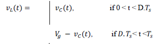
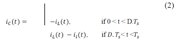
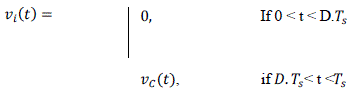
| Similar to a ZSI, the SBI also utilizes the shoot-through state of the H-bridge inverter (both switches in one leg of the Inverter are turned on simultaneously) to boost the input voltage to capacitor voltage .To explain the steady-state operation of the SBI, assume that the inverter is in shoot-through zero state for duration D.in a switching cycle . The switch S is also turned on during this interval. As shown in the equivalent circuit of Fig. 3(a),the inverter bridge is represented by a short circuit during this interval. The diodes Da and Db are reverse biased (as Vc >Vg ), and the capacitor C charges the inductor L through switch S and the inverter bridge. The inductor current in this interval equals the capacitor discharging current. For the remaining duration in the switching cycle (1 − D)., the inverter is in nonshoot- through state, and the switch S is turned off. The inverter bridge is represented by a current source in this interval as shown in the equivalent circuit of Fig. 3(b). Now, the voltage source Vg and inductor L together supply power to the inverter and the capacitor through diodes Da and Db. The inductor current in this interval equals the capacitor charging current added to the inverter input current. Note that the inductor current is assumed to be sufficient enough for the continuous conduction of diodes Da and Db for the entire interval (1 − D).Ts. | ||||||||||||||||||
| Fig. 4 shows the steady-state waveforms of the converter operation for one switching cycle Tswith respect to the gate signal Gsof switch S. From Fig. 3(a) and (b), one has | ||||||||||||||||||
 |
||||||||||||||||||
 |
||||||||||||||||||
 |
||||||||||||||||||
| Here,Vcand IL are dc components in Vc(t) and IL(t), respectively, and is the current drawn by the inverter bridge in the (1−D).TsInterval. Under steady-state, the average voltage across the inductor and the average current through the capacitor in one switching cycle should be zero. Using volt–second balance, we have | ||||||||||||||||||
| Similarly, | ||||||||||||||||||
| The average dc link voltage Vi can be calculated as | ||||||||||||||||||
| From equations (4)–(6), it can be observed that the expressions for the conversion ratios ( ,Vc /,Vg) and ( IL/ li) of SBI are the same as those for a ZSI, while the average dc link voltage of SBI is (1 − D) times that of ZSI.The switching states of SBI and ZSI are the same provided thatthe LC impedance network of ZSI is symmetrical. | ||||||||||||||||||
PWM CONTROL OF SBI |
||||||||||||||||||
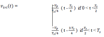
| In this paper, a modified PWM control strategy for the SBIis developed based on the traditional sine-triangle PWM withunipolar voltage switching [9]. In this scheme, the switch S willhave only two switching cycles perTs. Also, the switchingfrequency of S is always constant. Fig. 5 shows the schematic of the control circuit to generate the PWM control signal for the converter using the modified PWM control scheme, the gate controlsignals for switches S1 and S2 are generated by comparingthe sinusoidal modulation signals Vm(t) and −Vm(t) with a high frequency triangular carrier vtri(t) ofamplitude Vp. The frequency (fs) of the carrier signal is chosensuch that fs− fo Therefore, Vm(t)is assumed to be nearlyconstant during a switching cycle. The signals ST1and ST2 are generated by comparing vtri(t) with twoconstant voltages VSTand − VST , respectively. The purpose ofthese two signals is to insert the required shoot-through intervalD.TSIn the gate control signals of the inverter bridge. Now, thegate control signals for switches S1,S4 and S can be obtainedusing the logical expressions given as follows: | ||||||||||||||||||
| The resulting voltage waveforms at the input (Vi) and output (vAB) terminals of the inverter bridge. It can be observed that vAB has nine intervals in each switching cycle Ts. | ||||||||||||||||||
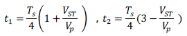
| a. Mathematical Relation Between V STand Shoot-Through Duty Ratio D | ||||||||||||||||||
 |
||||||||||||||||||
| Now, using equations (8) and (9), the expressions for t1and t2can be obtained as | ||||||||||||||||||
 |
||||||||||||||||||
| Substituting t1and t2in equation (9), the following can be obtained: | ||||||||||||||||||
 |
||||||||||||||||||
SIMULINK MODEL OF PWM GENERATION CIRCUIT |
||||||||||||||||||
| Fig. 5 shows the Simulink model for the modified unipolar PWM control strategy. The signals shown in Fig.8 provided to gates of the controllable switches S1−S2. VSTA DC signal controls the duration of shoot-through interval, hence adjust the duty cycle for the boost operation. Vm(t) Controls the modulation index for inverter operation. Fig. 11 and 12 shows the DC and AC output voltage waveform. DC voltage gain can be achieved by boost derived switched boost inverter is equivalent to boost converter, and is around four. | ||||||||||||||||||
SIMULINK MODEL OF BOOST DERIVED SWITCHED BOOST INVERTER |
||||||||||||||||||
| The boost derived switched boostinverter is derived from the switched boost inverter and boost converter. By replacingsingle switch in the boost converter by switched boost inverter we can derive boostderived switched boost inverter (BDSBI). Since SBI utilizes shoot through state inthe working, this state can be utilized for the working of boost converter. By varyingthe duty ratio of PWM control, the output AC and DC voltage can be adjusted.Same control scheme used for SBI can be used for BDSBI.For simulation of the proposed hybrid converter Parameters of the different circuit components are taken as: Input inductor (L) =5mH, DC capacitor (C) =1 mH, AC filter inductor Lac=4.6μH, AC filter capacitor (Cac) =50μF, DC load Rdc=20Ω, AC load Rac=25 Ω and Switching frequency is taken as 10 KHz [1]. | ||||||||||||||||||
SIMULATION RESULTS |
||||||||||||||||||
| A Simulink model of the SBI, along with the PWM control circuit of Fig.8 andFig.9, is designed and used to verify the proposed PWM technique and theoretical analysis given in the previous sections. Section V gives the parameters used for simulation ofthe SBI. For BDSBI, the output DC voltage can be varied from 281V(THD=0.7314) to 162V (THD=0.4314) and AC voltage from 140V (THD=0.01163)to 85V (THD=0.0584) from an input voltage of 100V for a variation of duty ratio(D) from 0.47 to 0. The duty ratio cannot be increased above 0.5. Table 4.1 showsthe DC and AC output voltages for different values of D. | ||||||||||||||||||
CONCLUSION |
||||||||||||||||||
| This paper proposes a new converter topology called boost derived switched boost inverter which can supply simultaneously both AC and DC load from a single DC source. Switched boost inverter which is derived from Z source inverter having better electromagnetic-interference, noise immunity when compared to a traditional voltage-source inverter (VSI) inherits all the properties of ZSI.The proposed boost derived switched boost inverter has the following advantages, shoot-through condition does not cause any problem on working of the circuit hence improves the reliability of the system, Implementation of dead time circuitry is not needed, Independent control over AC and DC output and the converter can also be adapted to generate AC outputs at frequencies other than line frequencies by a suitable choice of the reference carrier waveform. The output DC voltage can be varied from 281V to 162V and AC voltage from 140V to 85V for a variation of duty ratio (D) from 0.5 to 0. | ||||||||||||||||||
Tables at a glance |
||||||||||||||||||
|
||||||||||||||||||
Figures at a glance |
||||||||||||||||||
|
||||||||||||||||||
References |
||||||||||||||||||
|


