International Journal of Advanced Research in Electrical, Electronics and Instrumentation Engineering
ISSN ONLINE(2278-8875) PRINT (2320-3765)
ISSN ONLINE(2278-8875) PRINT (2320-3765)
Shantanu Krishna Mahato, C.vimala
|
| Related article at Pubmed, Scholar Google |
Visit for more related articles at International Journal of Advanced Research in Electrical, Electronics and Instrumentation Engineering
Cell phones are everywhere these days. It’s great to be able to call anyone at anytime. Unfortunately, restaurants, public places, class room, shopping malls and churches all suffer from the spread of cell phones because not all cell-phone users know when to stop talking while most of us just grumble and move on, some people are actually going to extremes to retaliate. Mobile jammer is a device used to prevent mobile phones from receiving or transmitting signals with the base stations. In this paper, we have to jam a cell phone, all we are developing a device that broadcasts on the correct frequencies. Although different cellular systems process signals differently, all cell-phone networks use radio signals that can be interrupted. GSM, used in digital cellular and PCS-based systems, operates in the 900-MHz, 1800-MHz and WCDMA 2100 bands in Europe and Asia and in the 1900- MHz band in the United States. Jammers can broadcast on any frequency and are effective against WCDMA, GSM and DCS. This project discusses the design and development of GSM Mobile jammer and aims to present a solution for the problems of occur through the cell phone. The main concept of jamming is the releasing of same frequency which is using by mobile service provider with noise so user equipment gets destruct.
Index Terms |
||
| Radio frequency, Triangular wave generator, Noise Generator, Power amplifier, Antenna. | ||
INTRODUCTION |
||
| Mobile jammer block mobile phone use by sending out radio waves along the same frequencies that mobile phones use GSM 900, DCS 1800, PSC 1900 and WCDMA 2100. This causes enough interference to block communication with mobile phones and towers for both GSM and WCDMA. GSM 900 has 25MHz bandwidth for uplink and 25MHz bandwidth for downlink. For jamming of GSM 900 Mobile we need generation of RF signal of these frequencies with sufficient power. Every Jamming Device outputs a Jamming Signal on one or more frequencies at a particular power. The Output Power of the Jammer can typically be stated in Watts or in some cases dBm. As with other radio jammer, cell phone jammers block cell phone use by sending out radio waves along the same frequencies that cellular phones use. This causes enough interference with the communication between cell phones and towers to render the phones unusable. Most cell phones use different bands to send and receive communications from towers. Jammers can work by either disrupting phone to tower frequencies or tower to phone frequencies. The radius of cell phone jammers can range from a dozen feet for pocket models to kilometers for more dedicated units[1]. | ||
| When I started my work on jammer, my aim was to design a jammer of low cost and effective jamming range. During search, I found lot of work has already been done. Design of both of jammers uses 2 RF amplifiers for power amplification. Use of 2 RF amplifiers increases the jamming range but it from also increases cost and complexity. In this paper I proposed Max2235 as a RF Amplifier which provides approximately same rang at the low cost and at less complexity[4]. | ||
JAMMER TECHNOLOGY |
||
| Five types of devices are known to have been developed (or being considered for development) for preventing mobile phones from ringing in certain specified locations[2]. | ||
| Type “A” Device (JAMMERS): This type of device comes equipped with several independent oscillators transmitting ’jamming signals’ capable of blocking frequencies used by paging devices as well as those used by cellular systems control channels for call establishment. | ||
| Type “B” Device (Intelligent Cellular Disablers): Unlike jammers, it does not transmit an interfering signal on the control channels. The device, when located in a designated ’quite’ area, functions as a ’detector’. It has a unique identification number for communicating with the cellular base station. | ||
| Type “C” Device (Intelligent Beacon Disablers): Unlike jammers, Type C devices do not transmit an interfering signal on the control channels. The device, when located in a designated ’quiet’ area, functions as a ’beacon’ and any compatible terminal is instructed to disable its ringer or disable its operation, while within the coverage area of beacon. | ||
| Type “D” Device (Direct Receive & Transmit Jammers): This jammer behaves like a small, independent and portable base station, which can directly interact intelligently or unintelligently with the operation of the local mobile phone. The jammer is predominantly in receive mode and will intelligently choose to interact and block the cell phone directly if it is within close proximity of the jammer. | ||
| Type E Device (EMI Shield - Passive Jamming): This technique is using EMI suppression techniques to make a room into what is called Faraday cage. Although labor intensive to construct, the Faraday cage essentially blocks or greatly attenuates, virtually all electromagnetic radiation from entering or leaving the cage - or in this case a target room[1]. | ||
EXPERIMENTAL DETAIL, METHODS & MATERIALS |
||
| Type A jammer is basically a transmitter which continuously transmits the signal of frequency range used by mobile/pcs system, but this type of jammer has drawback of continuous consumption of output power and continuous transmission of EMF signal in all directions without knowing that base station and mobile are trying to communicate with each other or not. It also creats | ||
| The effects of jamming depend on the jamming to signal ratio (J/S), modulation scheme, channel coding and interleaving of the target system. Generally Jamming to Signal ratio can be measured according to the following Equation[2]. | ||
| J/S = (PjGjrGrjRtrLrBr) /( PtGtrGrtRjrLjBj) | ||
| where: | ||
| Pj = jammer power | ||
| Pt = transmitter power | ||
| Gjr = antenna gain from jammer to receiver | ||
| Grj = antenna gain from receiver to Jammer | ||
| Gtr = antenna gain from transmitter to receiver | ||
| Grt = antenna gain from receiver to transmitter | ||
| Br = communications receiver bandwidth | ||
| Bj = jamming transmitter bandwidth | ||
| Rtr = range between communications transmitter and receiver | ||
| Rjt = range between jammer and communications receiver | ||
| Lj = jammer signal loss (including polarization mismatch) | ||
| Lr = communication signal lossThe GSM Air interface uses two different multiplexing schemes: TDMA (Time Division Multiple Access) and FDMA (Frequency Division Multiple Access). The spectrum is divided into 200 kHz channels (FDMA) and each channel is divided into 8 timeslots (TDMA). Each 8 timeslot TDMA frame has duration of 4.6 ms (577 μs/timeslot). Type A jammer consists of IF Section, RF Section, Antenna and Power supply. IF Section generate the intermediate frequency signals, frequency range of Intermediate signal of hundreds of Kilohertz. With the help of IF Section, RF Section generates the RF Signal. The frequency range of RF Signal is the range of GSM Signal range. For transmitting the RF Signal we need Antenna. Antenna covers both uplink and downlink frequency range[5]. IF Section consists of Triangular wave generator, RF Section consists of RF generator, RF power amplifier and Antenna. This project discusses the design and development of GSM Mobile jammer and aims to present a solution for the problems of occur through the cell phone. The main concept of jamming is the releasing of same frequency which is using by mobile service provider with noise so user equipment gets destruct[7]. | ||
| The noise generator TLO72CP which produce noise to the circuit. Without noise, the output of the VCO is just an un-modulated sweeping RF carrier. So, need to mix the triangular signal with to generate noise signal. Here used the Zener Diode operated in reverse mode and the triangle wave and noise signals are mixed using OP-Amp TL074[3]. | ||
| For generation of RF Signal I used Max2623 which is Voltage Controlled Oscillator capable of generation of 885- 960MHz signal. Input of this VCO is 0- 4.8 V Triangular wave signal. Frequency of triangular wave signal is 142 KHz. Generation of RF Signal of Mobile communication range does not give guarantee of disrupting the communication between the two parties; it needs more or equal jammer power at the mobile equipment, so we need amplification of RF Signal. here used Max2235 as RF Power Amplifier. Max2235 is a low voltage, silicon RF power amplifier designed for use in the 900MHz frequency band. It is capable to provide +32.5dBm output power. For transmitting the generated RF Signal I used λ/4 wave monopole GSM SMA Antenna, which can operate up to 2.4GHz[5]. | ||
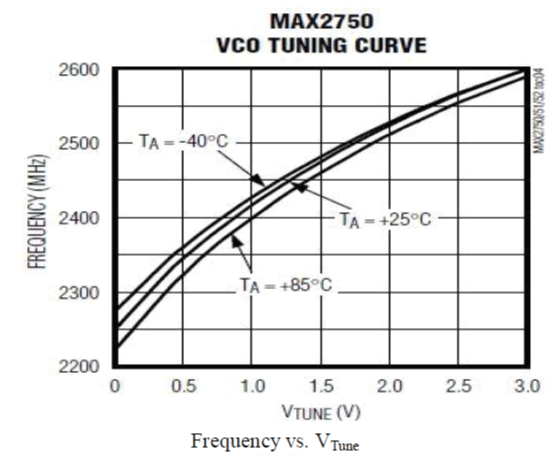
| The MAX2750/MAX2751/MAX2752 are selfcontained voltage- controlled oscillators (VCOs) intended for use in the 2.4GHz to 2.5GHz ISM band. Each IC combines a fully integrated oscillator and output buffer in a miniature 8-pin μMAX package[4]. | ||
| The inductor and varactor elements of the tank are integrated on-chip, greatly simplifying application of the part. The only required external components are a couple of supply bypass capacitors. The IC provides direct connection to the VCO tuning voltage input and the VCO buffer output. The tuning voltage input range is +0.4V to +2.4V, and the oscillator frequency tuning range is factory adjusted to provide guaranteed limits. The output signal is buffered by an amplifier stage (internally matched to 50Ω) to provide higher output power and isolate the device from load impedance variations. The MAX2750 operate over a +2.7V to +5.5V supply voltage range and the similar component MAXIM 303A Power amplifier for 2100 MHz. Internal regulation of the oscillator supply voltage eliminate the need for an external LDO regulator for the VCO[6]. | ||
| Max2623 is a Monolithic Voltage controlled Oscillator 8 pin IC. Pin no.2 is Oscillator Frequency Tuning Voltage Input, the output of IF section is applied at this pin. Pin no.3 has Ground Connection for Oscillator and Biasing; it requires a low-inductance connection to the circuit board ground plane. Pin no.4 is Shutdown Logic Input. A high impedance input logic level low disables the device and reduces supply current to 0.1μA. A logic level high enables the device. Pin no. 5 is Output Buffer DC Supply Voltage Connection. It requires Bypass with a 220pF capacitor to GND for best high- frequency performance. Pin no.6 is Bias and Oscillator DC Supply Voltage Connection. | ||
| It requires Bypass with a 220pF capacitor to GND for low noise and low spurious content performance from the oscillator. Pin No.7 is buffered Oscillator Output; output from this pin goes to RF amplifier for further amplification. Max2235 is a low voltage, silicon RF Power amplifier designed for used in the 900MHz frequency band. It operates directly from a single +2.7 to +5.5V supply. RF Power amplifier delivers +30dBm typical output power from a +3.6V supply or +28dBm from a +2.7 V supply. It can operate efficiently from -400C to +850C. We can see that even for -20dBm input power this RF amplifier provides +7dBm output power at 5V supply[7]. | ||
| The LTC1748 is perfect for demanding communications applications with performance that includes 76.3dB SNR and 90dB spurious free dynamic range. Ultralow jitter of 0.15psRMS allows under sampling of IF frequencies with excellent noise performance[4]. | ||
| Guaranteed Frequency Tuning Range:- | ||
| MAX2750: 2400MHz to 2500MHz (Zero IF) | ||
| MAX2751: 2120MHz to 2260MHz (240MHz to 280MHz IF) | ||
| MAX2752: 2025MHz to 2165MHz (335MHz to 375MHz IF) | ||
| ïÃâ÷ On-Chip Tank Circuit | ||
| ïÃâ÷ Internally Matched Output Buffer Amplifier | ||
| ïÃâ÷ Low-Current Shutdown Mode | ||
| ïÃâ÷ +2.7V to +5.5V Supply Voltage Range | ||
 |
||
 |
||
| To achieve the desired output power a gain stage was needed, about searching for asuitable power amplifier it is cheaper to use power amplifier from an old Mobile phones. The PF08103b Hitachi power amplifier module from Nokia mobile phone is sufficient to amplify an input signal in the range 800MHz to 1 GHz by 34 dB. But in the data sheet input should be 1dBm.To meet this requirement we use another 1748FA power amplifier stage after VCO. For this stage we use Mar-4SM power amplifier. The MAR-4Sm has a typical gain of 8-dB for the frequencies range from dc to 1GHz,so the output at this stage is around 5dBm[2]. | ||
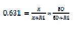
| For a 4-dB attenuation and symmetric Network S12=S21=0.631 | ||
| And for 50 ohms characteristic impedance we found the values of the resistor using the following equations, 50 = (R2 + 50) // (R3) + R1 | ||
 |
||
| Where X= (R2+50))//R3. | ||
ANTENNA |
||
| In order to have optimal power transfer, the antenna system must be matched to the transmission system. In this project, used two 1/4 wavelength monopole antennas, with 50 Ω input impedance so that the antennas are matched to the system. Here used monopole antenna since the radiation pattern is omni-directional for DCS 1800 antenna, 3G 2100 MHz antenna and GSM 900 antenna. | ||
| A monopole antenna is a class of radio antenna consisting of a straight rod-shaped conductor, often mounted perpendicularly over some type of conductive surface, called a ground plane. The driving signal from the transmitter is applied, or for receiving antennas the output signal to the receiver is taken, between the lower end of the monopole and the ground plane. One side of the antenna feedline is attached to the lower end of the monopole, and the other side is attached to the ground plane, which is often the Earth. This contrasts with a dipole antenna which consists of two identical rod conductors, with the signal from the transmitter applied between the two halves of the antenna. | ||
 |
||
RESULT |
||
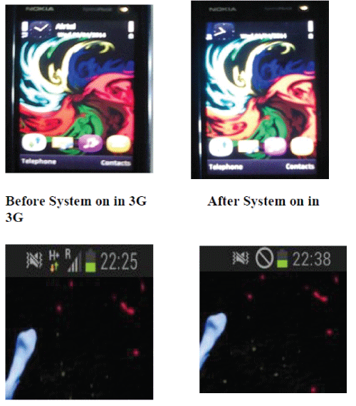
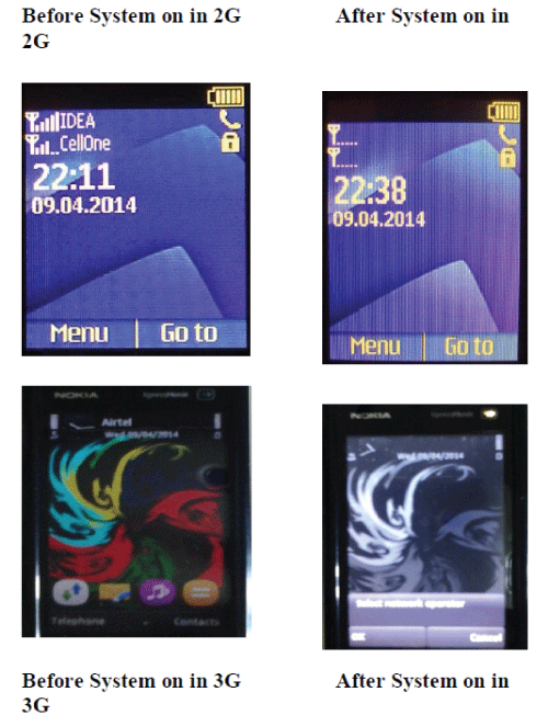
| Jammer blocked both 2G and 3G signas and tested with:- Airtel, Aircel, BSNL, Idea, Tata Docomo and Vodafone network. | ||
 |
||
 |
||
CONCLUSION & FUTURE WORK |
||
|
|
||
| Jamming technique is very useful to disable cell phone in a particular range so that it will not affect the other base station transmission system. Mobile jammer can be used in practically any location, but are used in places where a phone call would be particularly disruptive like Temples, Libraries, Hospitals, Jail, small Seminar hall etc. This project is designed partially till date and facing problem in power amplifier circuit design at which the frequency is matched, but not achieving proper output gain so that is can jam a particular signal for a particular range. | ||
| After blocking GSM 900, DCS (Digital Cellular Systems) 1800, PSC (Personal Communications Services) 1900 and WCDMA 2100 MHZ the next target is blocking of 4G system that is 2400 MHZ. Although the law clearly prohibits using a device to actively disrupt a cell-phone signal, there are no rules against passive cell-phone blocking. Companies are working on devices that control a cell phone but do not “jam the signal”. | ||
| In our busy life most of person use their mobile phone while drive which arise accidental possibility so in future to reduce accident the jamming system will operates whenever the driver turns on the ignition. The jamming device receives radiation emitted by the phone. The device can tell whether the mobile phone is being used by the driver or the passenger. Once the driver's use of cell phone is detected, a low-range jammer deactivates the cell phone without affecting other passenger’s cell phones and call wills dropped. | ||
Figures at a glance |
||
|
||
References |
||
|
