Keywords
|
| multilevel inverter, diode clamped inverter, induction motor, reverse mapping, space vector PWM. |
INTRODUCTION
|
| Multilevel inverters are the one,which can have a specify choice for various power application[1]-[3].Two level inverters waveforms are not smooth as the multi-level inverters. which can from different levels of the voltageDC. The most widely used techniques for implementing the pulse width modulation (PWM) strategy for multilevel inverters are sine-triangle PWM (SPWM) and space vector PWM (SVPWM) [4]–[14]. In multilevel SPWM, the reference sine wave is compared with a number of level-shifted carriers to decide the switches to be turned on [5]. In the SVPWM scheme, the sampled value of the reference voltage space vector which is the combined effect of the three-phase voltages is realized by switching the nearest voltage space vectors among the inverter voltage vectors [6]. There are different techniques available for implementing SVPWM for multilevel inverters [7]–[14]. In general, the SVPWM implementation involves the sector identification, switching-time calculation, switching-vector determination, and optimum-switching-sequence selection for the inverter voltage vectors [7]–[14]. The sector identification can be done by coordinate transformation [8], [9], [16] or by repeated comparison of the three phase reference voltages [7]. The lookup tables can be used for determining the switching vectors in optimum switching sequence [6]–[13]. The calculation of the duration of the switching vectors can be simplified using the mapping technique, in which the identified sector of the multilevel inverter is mapped to a corresponding sector of the two-level inverter [13]–[15]. SPWM can generate the SVPWM using the principle of equivalence with SPWM can generate the SVPWM signals directly from the instantaneous reference phase voltages for multilevel inverters . The fractal-based approach for SVPWM generation using a triangularization scheme to generate the voltage space vectors. |
PRINCIPLE OF THE PROPOSED METHOD
|
| The below diagram specifies a multilevel inverter(5).for simplicity the vectors are not depicted .due to adjacent vectors small triangles are formed are called sectors. Such six sectors around a voltage space vector forms a hexagon called sub hexagon [14], [15]. Multi-level inverters can be viewed as composed of a number of such sub hexagon. The shaded regions in Fig. 1 show two sub hexagons. They are represented as “sub hexagon I” (referred as inner sub hexagon) having the vector 000 as the center and “sub hexagon II” having the vector 330 as the center. The inner sub hexagon can be viewed as a space vector diagram of a two-level inverter whose inverter voltage vectors switch between the lowermost levels. Sub hexagon II can be also viewed as a space vector diagram of a two-level inverter, whose voltage vectors involve higher levels. The shifting of the sub hexagons in the space vector diagram of a multilevel inverter to the zero vector 000 simplifies the switching time calculations associated with multilevel inverters [13]–[15]. The shifting of sub hexagon II in the space vector diagram of a multilevel inverter toward the zero vector 000 involves the mapping of the sectors of sub hexagon II to the voltage space vectors associated with any sub hexagon By subtracting this vector at the center of the sub-hexagon, the reference space vector can be mapped. |
| Mapping related with different approach .the hexagon which is inside can be mapped to hexagon-II.due to addition vector space at the centre of hexagon II. Consider the voltage space vectors 000, 001, 101, and 111 associated with sector 5 of the inner sub hexagon and the voltage space vector 303 which is the vector at the center of sub hexagon II. Adding the voltage space vector 303 to the voltage space vectors associated with sector 5 of the inner sub hexagon gives the vectors 303 (000 +303), 304 (001+303), 404 (101+303), and 414 (111+303) which are the vectors associated with sector 5 of sub hexagon II. Similarly, the voltage space vectors associated with any sub hexagon can be generated by adding the vector at the center of the particular sub hexagon to the voltage space vectors of the corresponding sectors in the inner sub hexagon. In this paper, the mapping of the inner sub hexagon to any other outer sub hexagon (referred as reverse mapping) is used to generate the vectors associated with any sector in the space vector diagram of the multilevel inverter. |
| The generating switching vectors having instant vector space OT, the space vector reference OT lies in sector 1 to hexagon II.the centre of the vector (330) contain the reference tip vector space. By subtracting this vector at the center of the sub-hexagon, the reference space vector can be mapped as OT into sector 1 of the inner sub hexagon. The vectors 000, 100, and 110 are associated with sector 1 of the inner sub hexagon. By adding these vectors with the vector located at the center of sub hexagon III, the actual switching vectors 330, 430, and 440 for the reference space vector can be generated. Therefore, the actual sector that contains the reference space vector needs not to be identified for determining vectors to be switched by the inverter to realize the reference space vector. |
| In the proposed scheme, the vector at the center of the sub-hexagon is to be determined for the mapping of the reference whose voltage vectors involve higher levels. The shifting of the sub hexagons in the space vector diagram of a multilevel inverter to the zero vector 000 simplifies the switching time calculations associated with multilevel inverters [13]–[15]. The shifting of sub hexagon II in the space vector diagram of a multilevel inverter toward the zero vector 000 involves the mapping of the sectors of sub hexagon II to the sectors of the inner sub hexagon. This is done by subtracting the vector at the center of sub hexagon II from its other vectors. |
| The schematic proposed, where in the hexagon vector centre is enhanced to the mapping of reference vector space to hexagon –inner and for switching vector generation. Consider the voltage space vectors 000, 001, 101, and 111 associated with sector 5 of the inner sub hexagon and the voltage space vector 303 which is the vector at the center of sub hexagon II. Adding the space vector 303 to the voltage space vectors associated with sector 5 of the inner sub hexagon gives the vectors 303 (000 +303), 304 (001+303), 404 (101+303), and 414 (111+303) which are the vectors associated with sector 5 of sub hexagon II. Similarly, the voltage space vectors associated with any sub hexagon can be generated by adding the vector at the center of the particular sub hexagon to the voltage space vectors of the corresponding sectors in the inner sub hexagon. In this paper, the mapping of the inner sub hexagon to any other outer sub hexagon (referred as reverse mapping) is used to generate the vectors associated with any sector in the space vector diagram of the multilevel inverter.Fig. 2 shows the instantaneous reference space vector OT. The tip of the reference space vector OT lies in sec-tor 1 of sub hexagon III. The vector 330 is the center of sub hexagon III which contains the tip of the reference space vector. By subtracting this vector at the center of the sub-hexagon, the reference |
| space vector can be mapped as OT ̢̮̉ into sector 1 of the inner sub hexagon. The vectors 000, 100, and 110 are associated with sector 1 of the inner sub hexagon. By adding these vectors with the vector located at the center of sub hexagon III, the actual switching vectors 330, 430, and 440 for the reference space vector can be generated. Therefore, the actual sector that contains the reference space vector needs not to be identified for determining vectors to be switched by the inverter to realize the reference space vector. The switching vector and the sequence of the inner sub hexagon can be translated to the switching vector and sequence of the multilevel inverter by the proposed principle of reverse mapping. |
| Enhanced the principle with below |
| 1) Vector space of the inner hexagon mapping 2)Hexagon centre identification that contains reference vector space |
| 3)duration of switching vectors and optimum switching sequence using a two-level algorithm; |
| 4) Evaluation of the multiple switching vectors and maximum sequence switching using a two level algorithm. |
IDENTIFYING THE CENTER OF SUBHEXAGON
|
| The below diagram shows the multi-level inverters having different types of layers. These are the innermost layer (layer 1), the layer outside of layer 1 (layer 2), the next outer layer (layer 3), and the outermost layer (layer 4). These layers are represented as L1, L2, L3, and L4 in Fig. 2, and the instantaneous reference space vector OT is in layer 4 (L4). Layer 1 is the same as the inner sub hexagon mentioned in section II. The paper in which closest vector which is to reference vector space tip taken as hexagon centre. Among the vectors on the inner side of the layer, the vectors which belong to the 60âÃâæ region S3 are the most suitable vectors (candidate vectors) for the center of the sub-hexagon since this region contains the reference space vector. In this paper, these candidate vectors are automatically generated from the vectors of the inner sub hexagon, and the candidate vector which is closest to the tip of the reference space vector is chosen as the center of the sub hexagon. Therefore, in this paper, depending upon the layer of operation of the instantaneous reference space vector, all the candidate vectors for the center of the sub hexagon are generated, and the vector which is closest to the reference space vector is taken as the center of the sub hexagon. |
| III (A). Identifying the Layer of Operation |
| Vector space instantaneous reference can be solved into the axes ja, jb, and jc (Fig.2) using the following where va, vb, and vc are the instantaneous amplitudes of the three |
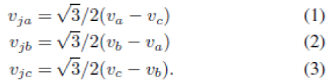 |
| The instantaneous reference space vector are lying in the 60 degree region will have maximum magnitude among these resolved values. |
| Let vj max be the maximum magnitude among the three resolved components. It may be noted that the width of each layer in the case of an n-level inverter is ((√3/2)(VDC/n − 1)). Therefore, the layer number can be easily obtained as |
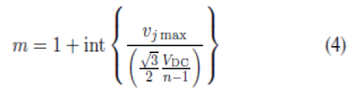 |
| Where m is the layer number |
| III.(B). Generating Candidate Vectors for the Subhexagon Center |
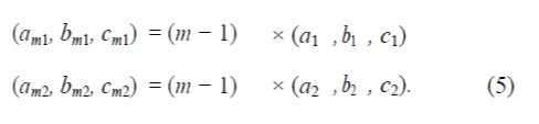
| Here the explanation which is mentioned vector space instantaneous reference in a specified m.so the hexagon centre of the candidate vectors on the inside of specified layer Fig. 3 shows a 60âÃâæ region in the space vector diagram of a five-level inverter. In the figure, the lines AB, CD, and EF are part of the inner sides of layers 2, 3, and 4, respectively. It may be noted that AB, which is the inner side of layer 2, is specify the layer inside vectors which is of two regions layer with any 60 degrees region(a1, b1, c1) and (a2, b2, c2) and the end vectors on the inner side of layer m be (am1, bm1, cm1) and (am2, bm2, cm2). Then, the end vectors on the inner side of layer m can be generated as |
 |
| The rest vectors which are in among final vectors can be generated by the differ vector (delta) (the difference between the end vectors of the inner sub hexagon) to the first end vector. The difference vector can be found out by subtracting the first end vector from the last end vector of the inner sub hexagon |
 |
| Repeated addition of the difference vector with the first |
| End vector on the inner side of layer m for m − 1 times can generate all vectors on the inner side of the layer m. Thus, all the vectors on the inner side of a particular layer can be automatically generated from the vectors of the inner sub hexagon. Of these candidate vectors, the vector which is closest to the reference space vector is chosen as the center of the sub hexagon containing the instantaneous reference space vector. The closest candidate vector can be easily determined by calculating a distance term “d” with respect to each of the candidate vector. The distance term indicates the distance of the candidate vector from the reference space vector. The distance term for the ith candidate vector can be calculated as |
 |
| Where the (vα, vβ) and (αcv , βcv ) are the coordinates of the reference space vector and candidate vector, respectively. The candidate vector with the smallest distance term is the vector closest to the reference space vector and hence taken as the center of sub hexagon. |
| For this process examine .the below figure vector space reference lying (4).within the S1 region. The inner side of layer 4 is EF. The vectors on the inner side of layer 2 in this case are 100 and 110, and the difference vector is 110 − 100 = 010. The end vectors of EF can be determined as 300 and 330 by multiplying 100 and 110 with 3 as per (5). The repeated addition of the difference vector three times to the first end vector 300 will generate the vectors 310 (300+010), 320 (310+010), and 330 (320+010) for the inner side of layer 4. |
| Of these candidate vectors on the inner side of layer 4, the closest vector to the reference space vector OT is 310, and it is chosen as the center of the sub hexagon associated with OT. |
| GENERATION OF SWITCHING VECTORS AND OPTIMUM SEQUENCE |
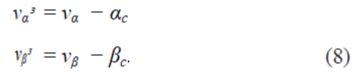
| Papers examines, by the principle of mapping the real vectors to be switched by the inverters are generated. Reference vector space which is contained by hexagon mapped to inside hexagon which is by removing of the located vector at the hexagon centre. For an n-level inverter, the inverting operation can be done by The two co-ordinates vector of the instantaneous reference space vector OT and (αc , βc ) is the coordinate of the center of the sub hexagon containing OT , the coordinates (vα |
 |
| Real switching vectors be translated by the two –level inverter vector by cross mapping, the switching vectors of the two-level inverter can be generated from the instantaneous amplitude of the phase voltages. The vectors of the two-level inverter can be translated to the actual switching vectors (corresponding to the multilevel inverter) by reverse mapping the inner sub hexagon to the sub-hexagon containing the tip of the reference space vector. This reverse mapping can be easily done by adding the vector at the center of the sub hexagon to the instantaneous switching vectors of the two-level inverter. If (a0, b0, c0) is the instantaneous switching vector corresponding to the two-level inverter and (ac, bc, cc) is the vector at the center of the sub hexagon, then the actual switching vector of the multilevel inverter is |
 |
| The above equation defines the cross mapping whereby the two-level inverter vectors are translated to the vectors of the multilevel inverter. Therefore, the actual vectors to be switched and the optimum sequence are automatically generated without using lookup tables. |
| In the description of previous example the diagram predicts the vector space reference OT mapped as OT ̢̮̉ to the inner sub-hexagon by subtracting the vector 310. Once the reference space vector is mapped to the inner sub hexagon, two-level SVPWM techniques can be employed for generating the two-level vectors in optimum sequence The twolevel inverter switching vectors in optimum sequence are determined using a two-level SVPWM technique, which will be similar to that of a conventional two-level inverter, i.e., 000 => 010 => 110 => 111 (Fig. 6). These two-level inverter vectors can be translated to the actual inverter voltage vectors of the multilevel inverter by the reverse mapping defined by (9). Since the center o. the sub hexagon is 310, the actual inverter voltage vectors to be switched are 310(000 + 310) => 320(010 + 310) =>420(110 + 310) => 421(111 + 310). |
SIMULATION OF PROPOSED METHOD FOR A MULTILEVEL INVERTER
|
| The proposed SVPWM method is implemented for a 4-kW 400 V.50 Hz three-phase induction motor for different modulation indexes. A three-level inverter motor drive configuration is used for the experiment (Fig 4). |
| A.Three-Level Inverter Configuration |
| Inverters using an induction motor configuration can realize multilevel inverter structures. The voltage across the phase winding of the induction motor can attain one of the three levels −VDC/2, 0, or +VDC/2, depending upon the switching states of the inverters. The switching combinations of inverter for realizing the different levels in the A-phase of a three-level inverter with IM configuration are shown in Table I, where S1u,S2u represent the top switches of Inverter and S3u,S4u represents the bottom switches, respectively, for the A-phase. |
| V.(B).Five Level Inverter Configuration |
| Inverters using an induction motor configuration can realize multilevel inverter structures. The voltage across the phase winding of the induction motor can attain one of the five levels –2Vdc,-Vdc 0,2Vdc or VDC, depending upon the switching states of the inverters. The switching combinations of inverter for realizing the different levels in the Aphase of a three-level inverter with IM configuration are shown in Table II, where Sa1,Sa2,Sa3,Sa4 represent the top switches of Inverter and Sa5,Sa6,sa7,sa8 represents the bottom switches, respectively, for the A-phase. |
| V.(C).Seven-Level inverter configuration: |
| Inverters using an induction motor configuration can realize multilevel inverter structures. The voltage across the phase winding of the induction motor can attain one of the seven levels −3VDC, −2VDC, −VDC, 0, +VDC, +2VDC, +3VDC depending upon the switching states of the inverters. The switching combinations of inverter for realizing the different levels in the A-phase of a three-level inverter with IM configuration are shown in Table III, where Sa1,Sa2,Sa3,Sa4, Sa5,Sa6 represent the top switches of Inverter and Sa7,Sa8,sa9,sa10, sa11,sa12 represents the bottom switches, respectively, for the A-phase,The below figure 6 represents seven level diode clamped inverter and the table III represents their switching states. |
| V.(D). simulation Experimental Results: |
| The SVPWM for the three-level inverter is implemented on a MAT LAB SIMULINK model . The experimental results are presented for different modulation indexes covering all layers of operation of the three-level inverter and the overmodulation region A dc link voltage of 130 V is used for each inverter (VDC/2).Graphs 1,2,3,4,5are shows the experimental results for a modulation index of 0.3 which corresponds to layer 1 (twolevel mode) operation. Graph 1(a) shows the plot of switching gate signal for 3-level, and graph.1(b) shows for 5-level switching gate signals, 1(c) shows for 5-level switching gate signals Graphs 2(a) and 2 (b ),2(c) shows the line voltages of Inverter .Graph 3(a),3(b),3(c)shows the performance of Induction Motor when fed to 3-level,5-level,7-level Inverter .Graphs 4(a),4(b),4(c) shows the waveforms of voltage THD for Induction Motor when fed to 3-level,5-level Inverter.Graphs 5(a),5(b) ,5(c) shows the waveforms of current THD for Induction Motor when fed to 3-level,5-level and 7-level Inverter. |
CONCLUSION AND COMPARISON
|
| A novel SVPWM scheme has been presented for multilevel inverters. The switching vectors and optimum switching se-quence are automatically generated by the principle of maping. The vector at the center of the subhexagon containing the reference space vector was directly identified in this paper reference space vector is mapped to the innermost subhexagon, and the switching vectors for the two-level inverters are generated. The two-level inverter vectors are translated to the vectors of the multilevel inverter by the principle of reverse mapping proposed in this paper. The SVPWM for any n-level inverter including an inverter with an even number of levels can be implemented without any additional complexity. The proposed SVPWM scheme is implemented on a MATLAB platform, and experimental results are presented for a three-level inverter and five level inverter and seven level inverter. |
| Comparisons: |
 |
 |
Tables at a glance
|
 |
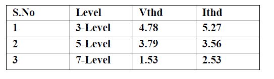
| Table 1 |
|
| |
Graphs at a glance
|
 |
 |
 |
 |
| Graph 1 |
Graph 2 |
Graph 3 |
Graph 4 |
 |
 |
 |
 |
| Graph 1a |
Graph 1b |
Graph 1c |
Graph 2a |
 |
 |
 |
 |
| Graph 2b |
Graph 2c |
Graph 4a |
Graph 4b |
 |
 |
 |
 |
| Graph 4c |
Graph 5a |
Graph 5b |
Graph 5c |
|
| |
References
|
- L. M. Tolbert, F. Z. Peng, and T. G. Habetler, “Multilevel converters for large electric drives,” IEEE Trans. Ind. Appl., vol. 35, no. 1, pp. 36– 44, Jan./Feb. 1999.
- J. Rodriguez, J.-S. Lai, and F. Z. Peng, “Multilevel inverters: A survey of topologies, controls, and applications,” IEEE Trans. Ind. Electron., vol. 49, no. 4, pp. 724–738, Aug. 2002.
- E. P. Wiechmann, P. Aqueveque, R. Burgos, and J. Rodríguez, “On the efficiency of voltage source and current source inverters for high-power drives,” IEEE Trans. Ind. Electron., vol. 55, no. 4, pp. 1771–1782, Apr. 2008.
- K. Zhou and D. Wang, “Relationship between space-vector modulation and three-phase carrier-based PWM: A comprehensive analysis,” IEEE Trans. Ind. Electron., vol. 49, no. 1, pp. 186–196, Feb. 2002.
- G. Carrara, S. G. Gardella, M. Archesoni, R. Salutari, and G. Sciutt , “A new multilevel PWM method: A theoretical analysis,” IEEE Trans. Power Electron., vol. 7, no. 3, pp. 497–505, Jul. 1992.
- H. W. Van Der Broeck, H.-C.Skudenly, and G. V. Stanke, “Analy-sis and realization of a pulsewidth modulator based on voltage space vectors,” IEEE Trans. Ind. Appl., vol. 24, no. 1, pp. 142–150, Jan./ Feb. 1988.
- N. Celanovic and D. Boroyevich, “A fast space-vector modulation al-gorithm for multilevel three-phase converters,” IEEE Trans. Ind. Appl., vol. 37, no. 2, pp. 637–641, Mar./Apr. 2001.
- P. F. Seixas, M. A. Severo Mendes, P. Donoso Garcia, and A. M. N. Lima, “A space-vector PWM method for three-level voltage source inverters,” in Proc. IEEE APEC, 2000, vol. 1, pp. 549–555.
- W. Yao, H. Hu, and Z. Lu, “Comparisons of space-vector modulation and carrier-based modulation of multilevel inverter,” IEEE Trans. Power Electron., vol. 23, no. 1, pp. 45–51, Jan. 2008.
- R. Beig, G. Narayanan, and T. Ranganathan, “Modified SVPWM algorithm for three level VSI with synchronized and symmetrical waveforms,” IEEE Trans. Ind. Electron., vol. 54, no. 1, pp. 486–494, Feb. 2007.
- Y.-H. Lee, B.-S.Suh, and D.-S. Hyun, “A novel PWM scheme for a three level voltage source inverter with GTO thyristors,” IEEE Trans. Ind. Appl.vol. 32, no. 2, pp. 260–268, Mar./Apr. 1996.
- B. P. McGrath, D. G. Holmes, and T. Lipo, “Optimized space-vector switching sequences for multilevel inverters,” IEEE Trans. Power Electron., vol. 18, no. 6, pp. 1293–1301, Nov. 2003.
- A. K. Gupta and A. M. Khambadkone, “A general space-vector PWM algorithm for multilevel inverters, including operation in over modulation range,” IEEE Trans. Power Electron., vol. 22, no. 2, pp. 517–526,Mar. 2007.
- J. H. Seo, C. H. Choi, and D. S. Hyun, “A new simplified space-vector PWM method for three-level inverters,” IEEE Trans. Power Electron. vol. 16, no. 4, pp. 545–550, Jul. 2001.
- J. Kim and S. Sul, “A novel voltage modulation technique of the spacevector PWM,” in Proc. Int. Power Electron. Conf., Yokohama, Japan, 1995, pp. 742–747.
|


