International Journal of Advanced Research in Electrical, Electronics and Instrumentation Engineering
ISSN ONLINE(2278-8875) PRINT (2320-3765)
ISSN ONLINE(2278-8875) PRINT (2320-3765)
Edwin Basil Lal1, George John P2, Jisha Kuruvila3
|
| Related article at Pubmed, Scholar Google |
Visit for more related articles at International Journal of Advanced Research in Electrical, Electronics and Instrumentation Engineering
Within the photovoltaic (PV) power-generation market, the ac PV module has shown obvious growth. However, a high voltage gain converter is essential for the module’s grid connection through a dc–dc boost converter. The converter is simulated with low dc voltage input for low power applications. A 15V input voltage, 200V output voltage, and 100W output power prototype circuit of the proposed converter has been implemented. The PV model implemented with MPPT algorithm using Perturb and Observe method is used with the boost converter to get the PV module. The PV module with booster developed will give a voltage gain range of 10-12 times the input voltage. The Comparative study between the normal booster PV model and high gain PV model is done. The simulation results are presented in this paper to verify the theoretical analysis by using software MATLAB
Keywords |
||||||||||||
| Photovoltaic(PV), Maximum power point tracking(MPPT), Perturb & Observe(P&O), Voltage gain, Ripple Factor. | ||||||||||||
INTRODUCTION |
||||||||||||
| Over the past few decades, the demand for renewable energy has increased significantly due to the disadvantages of fossil fuels and greenhouse effect .Among various renewable energy sources the most popular one is solar energy. Standalone PV system is the popular way of utilizing solar energy. PV panels are used to convert the solar energy into electrical energy without pollution. In the past few years, solar energy sources demand has grown consistently due to the following factors: 1) increasing efficiency of solar cells; 2) manufacturing technology improvement; and 3) economies of scale [1]. A major application of PV is in the area of distributed or dispersed generation (DG). DG facilitates injection of locally generated power into the grid. While DG has several advantages, it also has several challenges. As the capacity of PV system growing significantly, the impact of PV modules on power grid cannot be ignored. DG contains problems such as voltage variation, instability, interference, flicker, increase of harmonics and frequency drift etc. become more pronounced. Practical problems associated with the interaction of the PV system with the grid are the quality of power delivered to grid i.e. the power quality problems. Among these problems harmonics is found to be most important issue for grid interconnected PV system [2]. The output power produced by photovoltaic modules is influenced by the intensity of solar cell radiation, temperature of the solar cells and so on. When the quantity of this kind of power output is large enough, voltage pulsation on transmission lines will be obvious and difficult to control. Most of the renewable energy sources are connected to the grid by means of inverter. It is reported that the inverter supplies power of low quality at low level of solar radiation [3]. Under such conditions the PV array power and the corresponding inverter input power are low. For reducing harmonics in grid connected PV system several methods have been analysed. | ||||||||||||
| In this paper, firstly a PV module is designed with MPPT for the maximum working efficiency under any irradiance changes and temperature variations [4]. In a PV modelling systems the main problem is the voltage input of PV will be small when the irradiance level is low so this paper deals with a high step up voltage gain converter that can work with a voltage gain of 10-12 times the input voltage [5]. The converter will be highly useful in low irradiance condition for the working of low power appliances having a power output of 110W. The normal available booster circuit will provide a low voltage gain so the comparative study between this two converter is done and results are simulated for the easy selection of converter according to the irradiance and temperature availability. | ||||||||||||
MODELLING OF CONVERTER |
||||||||||||
| The circuit of a converter is shown in the fig 1. This converter provides a voltage gain of 10 times the input voltage with a low duty ratio (55%) and turns ratio (5). The boost is done by the inductor charging and discharge but it varies with change in duty cycle. This is done by 5 modes of operations. | ||||||||||||
| This converter has 5 modes of operations. The modes of operation are analysed in DCM. The operation of booster is almost same as the conventional booster circuit. The charging of coupled inductor and Lm gives high stored energy to the input voltage to get a high gained voltage. This converter is also simulated with Photo voltaic input in the later parts of this paper. | ||||||||||||
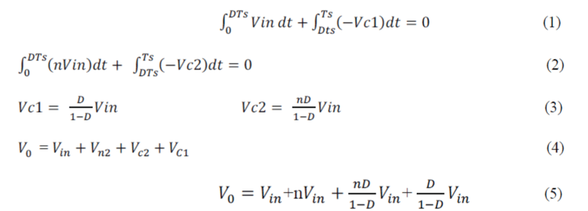
| In the converter applying a volt-second balanceequation , | ||||||||||||
 |
||||||||||||
| Vin= Voltage input,Vc1,Vc2=Voltage across Capacitor C1 and C2,Vn2=Voltage across inductor N2,Vo=Voltage output . From the 5thequation, The output voltage we can be varied according to the input voltages by changing the duty ratio(D).The effect of Duty ratio changes that happens to the system is analysed in the simulated model of converter. | ||||||||||||
SIMULATION OF HIGH GAIN CONVERTER |
||||||||||||
A. High Gain Converter |
||||||||||||
| The High gain booster circuit is implemented using matlab with parameter values C1=C2=47μFC3=220μF LOAD = 800 ohm Lm=30.54μH, turns ratio=5 duty ratio = 55%.This converter at this duty ratio gives more than 10 times the input voltage as output voltage( Vin=15V and Vout= 200V ) | ||||||||||||
B. High Gain Converter With PV Modelling |
||||||||||||
| The PV model is simulated with MPPT logic of perturb and observe to connect to the high voltage gain converter for the simulation checking with Vin= 20V and Vout = 228Vso the PV modelled with booster also give a high again more than 10 times with same parameter conditions. | ||||||||||||
SIMULATION RESULTS |
||||||||||||
A. Simulation Of High Gain Converter |
||||||||||||
| The above waveforms shows the charging currents voltages across the capacitors , diodes and inductors . The charging path will show the 5 modes of operations of the high gain converter to get the 10 times output voltage. | ||||||||||||
| Vd1 = Voltage across diode D1,Vo= Output Voltage, Io=Output current ,Po = Power output. | ||||||||||||
| The above waveforms shows the output value of voltage is boosted more than 10 times the input voltage with low power outputs of 60W to 100W with duty ratio changes that can be used for low power appliances even at low irradiance level. | ||||||||||||
| The high gain converter output is better in ripple comparison. The value of ripple is less than 1V in high gain converter but in normal converters it’s having a ripple output of 5V. | ||||||||||||
| The comparative study between the converters are done and the advantages of high gain converter is listed in table to illustrate the effectiveness of the new converter. | ||||||||||||
CONCLUSION |
||||||||||||
| This paper focuses on a new booster circuit implemented for low power appliances (110W).The high gain booster circuit modeling is done with normal dc input then the simulated waveforms are analyzed to model the booster with PV with MPPT logic. The waveforms of the normal PV output with normal booster areanalyzed to see the comparative study between this two. The results of the comparative study show the importance and practical advantages of high gain converter selection in PV modeling. Finally, the simulated outputs show the effectiveness of high gain converter than the low gain converter for selecting especially in PV modelling. | ||||||||||||
Tables at a glance |
||||||||||||
|
||||||||||||
Figures at a glance |
||||||||||||
|
||||||||||||
References |
||||||||||||
|


