International Journal of Advanced Research in Electrical, Electronics and Instrumentation Engineering
ISSN ONLINE(2278-8875) PRINT (2320-3765)
ISSN ONLINE(2278-8875) PRINT (2320-3765)
S.Divya1, Mrs.Vedavalli Prabhu2
|
| Related article at Pubmed, Scholar Google |
Visit for more related articles at International Journal of Advanced Research in Electrical, Electronics and Instrumentation Engineering
This paper deals with high boost voltage inverters that improve upon conventional Z-Source inverters. The conventional Z-Source inverter has an impedance network for buck-boost function to interface the DC source and inverter bridge. This proposed Improved Trans-Z-Source inverter has a transformer to obtain high voltage. This proposed inverter has increased voltage boost gain, reduced voltage stress and high boost factor due to the use of transformer. We can able to obtain high voltage from this inverter by making the turn’s ratio of the transformer more than unity. This paper presents the operating principles, analysis and simulation results of Improved Trans-Z-Source inverter and compares with the conventional Z-Source inverter. Both the shoot-through states and the turn’s ratio can be regulated to control the boost voltage gain. Index Terms-shoot through state, boost voltage gain, Improved Trans-Z-Source inverter
Keywords |
| The Z-Source inverter was introduced in order to accomplish single-stage power conversion with a buck-boost facility. In the conventional inverter when both the switches in the leg is turned on at same time the transferred energy causes huge voltage spike, in because the parasitic capacitances of the switches are too small compared to the amount of the transferred energy to them. The switches will get damaged because the voltage spike exceeds the break down voltage. This fact will decrease the reliability of the inverter. But in Z-Source inverter[1] this shoot-through states is effectively utilised and the realibity is increased and the output waveform distortion is reduced. This Z-Source inverter increases the immunity against the EMI problem which causes misgating of switches. But the Z-Source inverter undergoes many disadvantages such as less voltage gain, high voltage stress. |
| In order to improve the voltage gain we introduce a transformer which interface the DC source and the inverter bridge. This paper is performed under constant boost controls, which reduces the frequency ripples, reduce the inductor and capacitor requirement, and yet has slight voltage gain than maximum boost control. The transformer rating of the Improved Trans-Z-Source inverter is less compared to Trans-Z-Source inverter[8]. The lower the transformer power rating, the smaller the core size is. Therefore, the size and rating of the transformer is reduced. The improved inverter adds one inductor and capacitor with the transformer to obtain the high voltage gain. Thus this improved inverter has high reliability, high voltage gain, less stress. Therefore by increasing the turn ratio of the transformer, the voltage gain is increased. Thus a high voltage flows across the inverter bridge. |
II. CONVENTIONAL Z-SOURCE INVERTER TOPOLOGY |
| Fig. 1 shows the conventional Z-Source inverter topology. It employs a unique impedance network to couple the converter main circuit to the DC source, to the load or to any other converter circuit to provide unique features of buck-boost ability which cannot be observed in the conventional voltage source and current source inverter which has capacitor and inductor respectively. Another feature of the Z-source inverter is that the output ac voltage can be any value between zero and infinity. The Z-Source inverter consists of a split-inductor L1 and L2 and capacitorsC1 and C2 connected in X shape[7] is employed to provide an impedance source (Z-source) coupling the inverter to the dc source, load, or another converter. The dc source can be either a voltage or a current source. Therefore, the dc source can be a battery, diode rectifier, thyristor converter, fuel cell, an inductor, a capacitor, or a combination of those. Switches used in the converter can be a combination of switching devices and diodes such as the antiparallel combination. |
| The three-phase Z-source inverter bridge has nine permissible switching states unlike the conventional three-phase voltage source inverter that has eight. The conventional three-phase voltage source inverter has six active vectors when the dc voltage is impressed across the load and has two zero states when the load terminals are shorted through either the lower or upper three devices, respectively. However, the three-phase Z-source inverter bridge has one extra zero state when the load terminals are shorted through both the upper and lower devices of any one phase leg (i.e., both the devices are gated on), any two phase legs, or all three phase legs. This shoot-through zero state is forbidden in the conventional voltage source inverter, because it would cause a shoot-through. We call this third zero state as shoot-through zero state, which can be generated by seven different ways. This shoot-through states is effectively utilised to provide the buck-boost facility. |
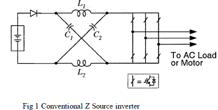 |
| During the zero states all the switches in the upper or lower side are shorted. At this state the inductor L1 and L2 gets energised. When the diagonal switches conducts this stored charge in inductor will transferred across the switches. Yet when the switches in the same leg conducts simultaneously this stored charge will get transfered to the capacitor C1 and C2. Thus voltage spikes across the switches are avoided which will prevent the switches from damages. |
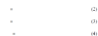
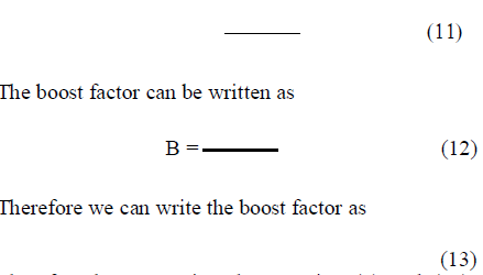
| The ratio between the DC link voltage across the inverter bridge and the input DC voltage is boost factor of Z- source inverter and can be written as |
| Where D=T0/T is the duty cycle of each shootthrough state.T0 is the shoot-through interval during the switching interval, T is the total time period. Note that the shoot-through state does not affect the output voltage because the shoot-through state’s ouput voltage is zero which is similar to null state. Thus without affecting the active states the shoot-through states are evenly allocated in the total time period. |
| Even though the Z-source inverter overcomes the conceptual and theoretical barriers and limitations of the traditional voltage-source and current-source inverter and provides a novel power conversion concepts it suffers from many disadvantages. |
| 1) The input DC current is discontinuous in ZSource inverter and has high ripple in the output voltage. |
| 2) High voltage stress across the switches |
| 3) It has less voltage boost factor which is not sufficient in high power application. |
| Thus the above disadvantage can be overcome by the Improved Trans-Z-source inverter. |
III. PROPOSED IMPROVED TRANS-ZSOURCE INVERTER |
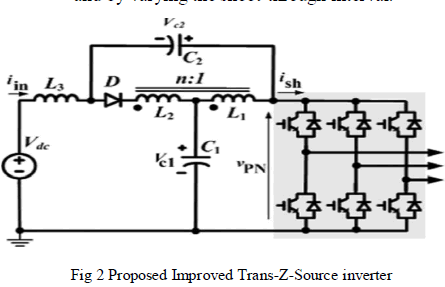
| Fig.2 shows the proposed Improved Trans-Z-Source inverter with continuous input current and with buckboost capability. It is created by connecting a transformer with the inductor and a capacitor between the DC source and the inverter bridge. Thus the proposed inverter consists of a one inductor L3, one transformer, two capacitor C1 and C2, and one diode D. The main characteristics of this inverter are |
| 1) Input current is continuous |
| 2) Higher boost factor can be obtained |
| 3) The voltage buck-boost can be possible by increasing the turns-ratio of the transformer and by varying the shoot-through interval. |
 |
A. Operating Principles |
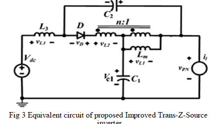
| The Proposed Improved Trans-Z-Source inverter has extra shoot-through zero states in addition to the conventional six active and two zero states in a conventional voltage-source inverter. The operating principles of the improved inverter are similar to those of the conventional Z-source inverters. For the purpose of analysis, the operating states are simplified into shootthrough and non shoot-through states. Fig. 3 shows the equivalent circuit of Improved Trans-Z-Source inverter with a mutual inductance. |
 |
B. Modes of Operation |
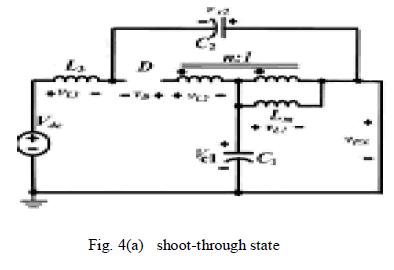
| 1) Mode 1: In the shoot-through state as shown in Fig. 4(a),the inverter side is short circuited by both the upper and lower switching devices of any of the phase leg. During this shoot-through state, the diode D is reverse biased (i.e) D is OFF. |
 |
| During the shoot-through state |
 |
| During shoot-through states the inductor L3 gets energised. Due to short circuit, heavy current flows through the transformer winding L1. Due to this winding L1, the winding L2 also gets energised due to coupling. The capacitor C1 also gets energised. |
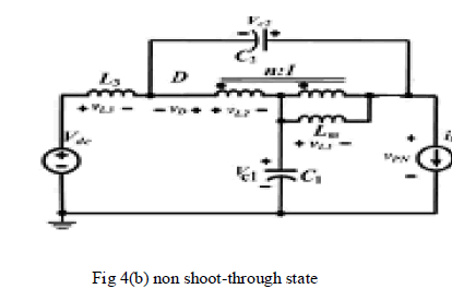
| 2)Mode 2:In the non-shoot through states as shown in Fig. 4(b), the improved inverter has six active states, and two zero states of the main circuit. During the non-shootthrough state the diode D is forward biased. The corresponding voltages across the primary and secondary winding of the transformer in the non-shoot-through states are and respectively. |
 |
| During non-shoot-through states the capacitor C2 gets charged through transformer. Then the diode D forward biased through which the transformer winding gets energized. Thus the main power flowing through to the inverter bridge is the total power from the transformer and the capacitor C2. |
 |
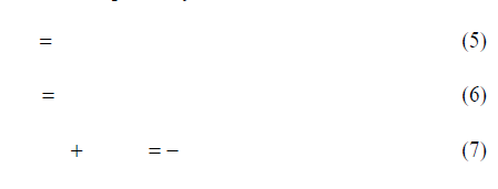
| Applying the volt-second balance principle to inductor L1 and L2 (1) and (2). Thus we obtain |
 |
| The peak dc-link voltage across the inverter bridge can be written as |
 |
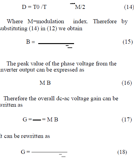
| Therefore by comparing the equation (1) and (12) the Improved Trans-Z-Source inverter has higher boost factor than the conventional Z Source inverter by the use of transformer. When n = 0, the Improved Trans-Z-Source inverter will work normally as a conventional Z Source inverter. But when n≥1 the boost ability of the Improved Trans-Z-Source inverter is higher and can be increased by increasing the turns ratio of the transformer. On the other hand this Improved Trans-Z-Source inverter uses a smaller shoot-through duty cycle to produce the same boost factor as the conventional Z Source inverter. Thus a higher modulation index is used to have a better output waveform. |
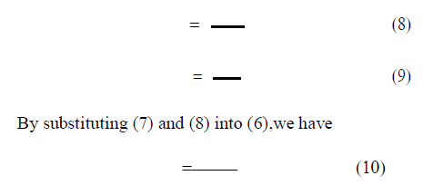
| When we use constant boost control[2],the constant duty cycle of the shoot-through state of this inverter can be written as, |
 |
| The proposed Improved Trans-Z-Source inverter incurs a lower voltage stress on the dc link, a lower current stress flow to the transformer windings and diode, and a lower input current ripple. However, the voltage stress on the diode and the current stresses across the main power circuit during the shoot-through state of the Improved Trans-Z-Source inverter are higher. This is because the Improved Trans-Z-Source inverter has a stronger power capability at the high modulation index. |
C. Comparisons of Constant boost control, simple boost control and maximum constant boost control |
| The gate pulses are obtained in simple boost technique but the drawback of the method is that it cannot be used for boosting the output voltage to a higher extent because of constant maintaining of shoot through time per switching cycle. Voltage stress in switches increases as the voltage gain increases. So, this control method[6] cannot be implemented to obtain higher gain because of the limitation of voltage ratings of the switches. Therefore, other suitable control techniques can be adopted to operate the Z-source inverter at higher voltage gain. |
| Voltage stress is minimized on switches by aximizing shoot through and boost factor. Considering the simple boost control method, a simple modification is required. The voltage stress is much lower in comparison to the simple boost control. |
| Hence, the inverter can be operated at a higher voltage gain. In this method all the zero states are utilised as shoot through states hence a maximum output is produced from is method. This method introduces a low-frequency current ripple that is associated with the output frequency in the inductor current and the capacitor voltage. This will cause a higher requirement of the passive components when the output frequency becomes very low. Therefore, the maximum boost control is suitable for applications that have a fixed or relatively high output frequency and the six-time frequency current ripple is not a problem. For applications with variable and low output frequency, the method may require a large dc inductor. |
| Therefore in order to overcome the above drawbacks such as voltage stress, low frequency ripples and to reduce the inductor and capacitor requirement so that volume and cost of the network is reduced, we so introduce the constant boost control method. Therefore to reduce the volume and cost of the Z-source network, we need to eliminate the low-frequency current ripple by using a constant shoot-through duty ratio. At the same time, a greater voltage boost for any given modulation index is desired to reduce the voltage stress across the switches. More importantly, the constant boost control method requires the minimum inductance and capacitance because the inductor current and capacitor voltage contains no low-frequency ripples associated with the output voltage, thereby reducing the cost, volume, and weight of the Z-source network. The voltage stress is reduced compared to simple boost control and slightly more than the maximum constant boost control. The input current is the current flows through the inductor L3. Thus the input current ripple in the Improved Trans-Z-Source inverter is negligible and equal to zero. |
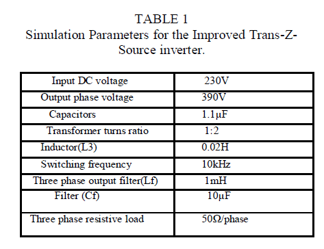
IV. SIMULATION RESULTS |
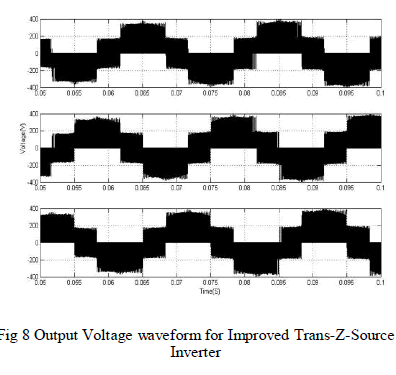
| ïÃâ¬Ã Ã¯ÃÂÃâo verify the advantage of the proposed Improved Trans-Z-Source inverter shown in Fig. 2, MATLAB simulation compares its performance with the conventional Z Source inverter[1]. The input voltage is chosen to be 230 and the output phase voltage is to be 390 . Constant boost control is used. The TABLE I shows the simulation parameters for the inverter. The filter is used to reduce the distortion in output waveform. |
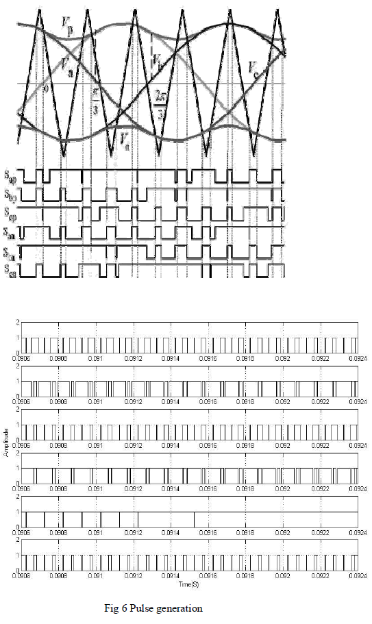
| The gate pulses are provided to the switches by comparing the three reference wave with a carrier triangular wave. The gate pulse generation is the key source in this inverter. This shoot-through is implemented by constant boost control where a third harmonic injection wave is compared with the triangle were a pulse is generated. These pulses will provide a shoot-through by which, the switches in the same leg conducts. Fig 5 shows pulse generator by constant boost control. |
 |
| The modulation index is determined by comparing the amplitude of reference and carrier triangle. So the modulation index so chosen is M=0.96. Fig 6 shows the pulse generation of the constant boost control method. |
 |
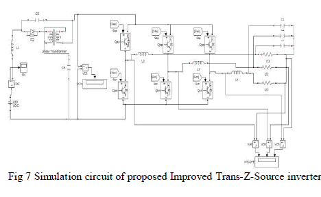 |
| Fig 7 shows the simulation circuit of the proposed improved Trans-Z-Source inverter. In this circuit we use a transformer to boost the dc link voltage. In this method the output voltage can be able to buck-boost the voltage by modifying the modulation index which will vary the shoot-through pulses. Thus the voltage is boosted by both the transformer and the capacitor. Fig 8 shows the output voltage of the Improved Trans-Z-Source inverter were the voltage is boosted to about 390V ac. By comparing the output voltage of Z-Source inverter of 240V, this proposed inverter has higher boost voltage of 390V, rather than this proposed inverter has higher boost voltage gain, continuous input current, less voltage stress. |
 |
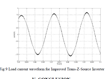
| Fig 9 shows the load current of the improved Trans-Zsource inverter. The total harmonic distortion is measured in the load current. The distortion factor of the proposed Improved Trans-Z-source inverter is 2.36% which is very much less compared to the conventional Z-Source inverter is 7.42%. |
 |
V. CONCLUSION |
| Thus a new topology was designed to improve the conventional Z Source inverter with the following characteristics such as high boost voltage, buck boost is possible by varying the shoot through interval and also by varying the transformer turn ratio, and the input current is continuous. Compared with the conventional Z-source inverters, for the same input voltage the improved Trans- Z-Source inverter has a higher boost output voltage, reduced voltage stress on the dc link, lower current stress flow to the transformer windings, and lower input current ripple. |
| The simulation results for input voltage of 230V DC we obtain the output of about 390V AC output voltage. This improved Trans-Z-Source inverter is applicable to fuel cells, photovoltaic application where the obtained output voltage should be boosted to high AC voltage. |
References |
|