Index Terms
|
| phase-shedding operation, switched mode rectifier |
INTRODUCTION
|
| The qualified AC/DC conversion must meet the functions of input current shaping and output voltage regulation. The boost-type switch-mode rectifier (SMR), including a diode rectifier and a boost converter, is often used to perform the qualified Ac/Dc conversion. The conventional boost-type SMRs, the multiphase SMRs with an interleaved control scheme possess smaller current ripples and higher efficiency. Interleaving operation can be adopted to increase the power capacity, while still keep low current or voltage ripple. Due to the wide utilization of ac/dc power supply in electric systems, the problem of input harmonic current has been a big concern. This leads to the demand for electrical equipments to comply with the European Norm EN61000-3-2. Boost power factor correction (PFC) regulator has been used as a popular solution to suppress current harmonics, achieve unity power factor (PF), and utilize full line power [1]-[3]. To meet efficiency requirements, more and more multiphase boost-type SMRs were used in fuel-cell power-generation systems [4], Electric vehicle (EV) power conditioning systems usually utilize a high-energy battery pack to store energy for the electric traction system [5], and photovoltaic applications [6]. Therefore, more and more research has focused on multiphase boost-type SMRs. Thus results [7]-[9] the lightload system efficiency can also be significantly improved by shutting down some boost cells (i.e., phase-shedding operation). Besides the phase-shedding technique, several other techniques are used to improve the light load efficiency of Dc–Dc converters such as pulse skipping, constant ON time techniques, mode hopping, or pulse frequency modulation. These techniques are suitable in lower load current applications such as a point of load (POL) converter or portable devices. However, these techniques do not fully take the thermal characteristics of semiconductor components into account to optimize the performance. It is designed by using a digital tool as a fieldprogrammable gate array (FPGA); therefore, the operation for phase shedding is flexible, but the load switching point is not optimized because of the power loss is not involved in that method. |
N-PHASE BOOST-TYPE
|
| Fig. 1 shows the topology of an N-phase boost-type SMR, where integer N is the topology phase number (N>1). It consists of a diode bridge rectifier, N boost converters with the identical inductors and the identical diodes. To model the behavior of the N-phase boost-type SMR, some assumptions are initially made: 1) All switches are assumed to operate at a fixed period much smaller than the line period and thus, the input voltage over one switching. Period can be seen as a constant, and 2) a bulk capacitor is connected to the output dc voltage, and thus, the output voltage is assumed to be equal to its average value. |
| According to KCL, the total inductor current iL is the sum of individual inductor currents |
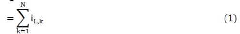 |
| When the input voltage vs(t)=Vsp sin (2πt/T)= Vsp sin(ωt) is positive, the total inductor current iL is equal to the input current is, and the current iL is equal to the negative input current is when the input voltage vs turns to negative.The input current can be represented in terms of the total inductor current iL . |
DESIGN OF INDUCTOR
|
| To consider the practical condition, the nonzero inductor resistors are assumed. In addition, the effects of the voltage drops across the diode bridge rectifier, the freewheeling diode, and the semiconductor switch are also considered. The total voltage drop in the “switch-on” path is the sum of the voltage drops across the bridge rectifier and the semiconductor switch is also Zero. |
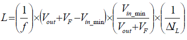 |
| The frequency is 25KHZ if the value chosen below that current value will goes to discontinuous mode within that half cycle. |
| Vout is the output voltage, Vf is the voltage drop across the diode 0.7 V MIN = minimum Voltage of the Boost SMR, VMAX = maximum Voltage of the Boost SMR |
| Therefore, from (2), the behavior of the average total inductor current with the active-phase number n in an Nphase boost-type SMR can be equivalently modeled by a boost-type SMR, as shown in Fig. 2. |
DESIGN OF PROPORTIONAL CONTROLLER
|
| The proposed method can be seen as a proportional–integral (PI)-type voltage controller illustrated in Fig. 3 |
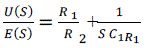 |
| U(S) = Output current |
| E(S) = Input current |
| R1 = feedback resistor |
| R2 = Input resistor. |
| C1 = Filter capacitor |
| A. Design of the Differentiator |
| It is crucial to design a differentiator that can extract inductor voltage accurately. In addition, the differentiator should be ca- pable of attenuating undesirable highfrequency component in and the injected noise, because derivative function is usually sensitive to high-frequency signals. |
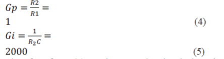 |
| Therefore from (4) Gp is proportional gain here both the resistors value is 10 Ω. From (5) Gi is integral gain value is 10 Ω and 0.5mF. To avoid the effect of the double-linefrequency voltage ripple in the output voltage, the cutoff frequency is chosen to be smaller than the 1/20 of the double line frequency is proposed in this design. |
PHASE-SHEDDING OPERATION
|
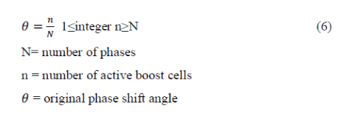
| At light load, more than one boost cell should be shut down to reduce the total switching loss and to increase the lightload efficiency. To work well under the phase-shedding operation, an adjustable gain (N/n) was included in this method. It is able to reduce the voltage dip due to the phase- shedding operation. |
 |
SIMULATION RESULTS
|
| In this section, a series of the computer simulations is provided to demonstrate the proposed boost-type SMR. The nominal values and the circuit elements are listed in Table II. The controller parameters were chosen as Gp =1rad/V and Gi =2000 rad/V/s. The simulation is done by using Psim software. |
| In fig.5. A single phase A.C. supply is given to the diode rectifier and current flows through the boost converter to the load output voltage is measured using voltage sensor. The input voltage is compare with zero detecting circuit and compared with the comparator .The output of the comparator compares the output from PI controller and given to ON-OFF controller. It provides the gate pulse for boost converter. |
| In Fig.6 (a) shows the output voltage single phase switched mode rectifier the average output voltage of the waveform is 390V. The above Fig.6 (b) shows the output current of single phase switched mode rectifier the average output current of the waveform is 1.3A. |
| In Fig 6(c) shows the pulse waveform for the Gate1 and Gate 2. Gate1 is ON for 0.02ms and Gate2 is ON for the next 0.04ms here the switching stress will be high because of continuous triggering pulses for both switches. |
| In Fig.7. A single phase A.C. supply is given to the diode rectifier and current flows through the boost converter to the load output voltage is measured using voltage sensor and output current measured using current sensor. The input voltage is compare with zero detecting circuit and compared with the comparator .The output of the comparator compares the output from PI controller and given to AND gate. The output of current sensor is given to the comparator output of AND gate is also compared with that comparator and if both inputs are high the switches will ON if it is low it will OFF. This is phase shedding operation In Fig.7 (a) here the Gate 1 is on and Gate 2 is off so switching loss will be reduced overall efficiency will be increased. |
| In fig.8. A single phase A.C. supply is given to the diode rectifier and current flows through the boost converter to the load output voltage is measured using voltage sensor and output is given to PI controller and that output is given to the JK flip-flops and given to phase shedding operation to trigger gate pulse for boost converter. |
| When J=0, K=0 the output of the NAND gate corresponding to J becomes 0 .Therefore Q becomes 0. This condition will reset the flip-flop. This represents the RESET state of Flip-flop. |
| When J=1, K=0In this case, the NAND gate corresponding to K becomes 0.Therefore Q becomes 0. This condition will set the Flip-flop. This represents the SET state of Flip-flop. |
| When J=K=1In this case, J=K=1. This will cause the output to complement again and again. This complement operation continues until the Clock pulse goes back to 0. |
| In Fig.8 (c) here the Gate 1,2 is on and Gate 3,4 is off so switching loss will be reduced overall efficiency will be increased. Power loss in that overall circuit is also reduced. |
| In Fig.9. A three phase A.C. supply is given to the diode rectifier and current flows through the boost converter to the load output voltage is measured using voltage sensor and output current measured using current sensor. The input voltage is compare with zero detecting circuit and compared with the comparator .The output of the comparator compares the output from PI controller and given to AND gate. The output of current sensor is given to the comparator output of AND gate is also compared with that comparator and if both inputs are high the switches will ON if it is low it will OFF. This is phase shedding operation. |
| Figure 9(a) shows the output voltage waveform of three phase switched mode rectifier the average output voltage of the waveform is 420V. |
| Fig.9 (b) output current waveform of three phase switched mode rectifier the average output current is 1.4A . In Fig.9 (c) here the Gate 3 is on and Gate1and 2 is off so switching loss will be reduced overall efficiency will be increased. |
CONCLUSION
|
| The control of single phase and three phase SMR with phase shedding operation has been discussed and simulated. The proposed system has demonstrated very good performance with reduced switching losses and lesser number feedback signals and lesser number of sensors is used. Overall efficiency will be increased. |
Tables at a glance
|
|
|
Figures at a glance
|
 |
 |
 |
 |
 |
| Figure 1 |
Figure 2 |
Figure 3 |
Figure 4 |
Figure 5 |
 |
 |
 |
 |
| Figure 6 |
Figure 7 |
Figure 8 |
Figure 9 |
|
References
|
- J. M. Wang, S. T. Wu, Y. F. Jiang, and H. J. Chiu, “A dual-mode controller for the boost PFC converter,” IEEE Trans. Ind. Electron., vol. 58, no. 1, pp. 369–372, Jan. 2011.
- K. Yao, X. Ruan, X. Mao, and Z. Ye, “Variable-duty-cycle control to achieve high input power factor for DCM boost PFC converter,” IEEE Trans. Ind. Electron., vol. 58, no. 5, pp. 1856–1865, May 2011.
- F. Zhang and J. Xu, “A novel PCCM boost PFC converter with fast dynamic response,” IEEE Trans. Ind. Electron., vol. 58, no. 9, pp. 4207– 4216, Sep. 2011.
- W. Li, L. Fan, Y. Zhao, X. He, D. Xu, and B. Wu, “High-step-up and high-efficiency fuel-cell power-generation system with active clampflyback–forward converter,” IEEE Trans. Ind. Electron., vol. 59, no. 1, pp. 599–610, Jan. 2012
- M. Pahlevaninezhad, P. Das, J. Drobnik, P. K. Jain, and A. Bakhshai, “A ZVS interleaved boost AC/DC converter used in plug-in electric vehicles,” IEEE Trans. Power Electron., vol. 27, no. 8, pp. 3513–3529, Aug. 2011
- C. N. M. Ho, H. Breuninger, S. Pettersson, G. Escobar, L. A.Serpa, and A. Coccia, “Practical design and implementation procedure of an interleaved boost converter using SiC diodes for PV applications,” IEEE Trans. Power Electron., vol. 27, no. 6, pp. 2835–2845, Jun. 2012.
- X. Xu, W. Liu, and A. Q. Huang, “Two-phase interleaved critical mode PFC boost converter with closed loop interleaving strategy,” IEEE Trans. Power Electron., vol. 24, no. 12, pp. 3003–3013, Dec. 2009.
- M. Halton, “Efficiency-based current distribution scheme for scalable digital power converters,” IEEE Trans. Power Elec- tron., vol. 26, no. 4, 1261–1269, Apr. 2011
- J. T. Su and C. W. Liu, “A novel phase-shedding control scheme for improved light load efficiency of multiphase interleaved DC–DC converters,” IEEE Trans. Power Electron., vol. 28, no. 10, pp. 4742–4752, Oct. 2013.
|