International Journal of Advanced Research in Electrical, Electronics and Instrumentation Engineering
ISSN ONLINE(2278-8875) PRINT (2320-3765)
ISSN ONLINE(2278-8875) PRINT (2320-3765)
Nikhil Mohanan1, Daisykutty Abraham2, Geethu James3
|
| Related article at Pubmed, Scholar Google |
Visit for more related articles at International Journal of Advanced Research in Electrical, Electronics and Instrumentation Engineering
Power supplies with active power factor correction (PFC) techniques are becoming necessary to meet harmonic regulations and standards. Conventional PFC scheme has lower efficiency due to significant losses in the diode bridge. In an effort to maximize the power supply efficiency, considerable research efforts have been directed toward designing bridgeless PFC circuits, where the number of semiconductors generating losses is reduced by eliminating the full bridge input diode rectifier. A bridgeless PFC Rectifier allows the current to flow through a minimum number of switching devices compared to the conventional PFC rectifier. Accordingly, the converter conduction losses can be significantly reduced and higher efficiency can be obtained, as well as cost savings. Several bridgeless topologies, which are suitable for step-up/step-down applications have been introduced. The CUK converter offers several advantages in PFC applications. Unlike the SEPIC converter, the CUK converter has both continuous input and output currents with a low current ripple. Thus, for applications which require a low current ripple at the input and output ports of the converter, the CUK converter seems to be a potential candidate in the basic converter topologies. Due to the lower conduction and switching losses, the bridgeless CUK topology can further improve the conversion efficiency when compared with the conventional CUK PFC rectifier. To maintain the same efficiency, these circuits can operate with a higher switching frequency. It will reduce the size of the PFC inductor and EMI filter. The power factor value can be achieved up to 0.9136 using this circuit with a power of 166 W. It is proven by using MATLAB simulation.
Keywords |
||||||||||
| Bridgeless rectifier, CUK converter, low conduction losses, power factor correction (PFC) rectifier, total harmonic distortion (THD). | ||||||||||
INTRODUCTION |
||||||||||
| Power factor (PF) is defined as the ratio of real power to apparent power, where real power produces real work and apparent power is the product of RMS value of voltage and current. When PF is not 1, the current waveform does not follow the voltage waveform. This results in power losses and may also cause harmonics that travel down the neutral line and disrupt other devices connected to the line. The power Factor Correction (PFC) circuit basically shapes the input current waveform to be the replica of the input voltage waveform and exactly in phase with it. Active PFC is preferred to passive one because of its small form factor and much better PF. Active PFC [3] is usually based on dc-dc converter where the feedback control can be performed in continuous conduction mode (CCM), discontinuous conduction mode (DCM), or critical conduction mode (CRM). Converter that operates in CCM induces small device current stress and the requirement on input filter is relaxed. However, the hard turn-OFF of freewheeling diode increases power loss and switching noise. DCM is commonly used for low-power application. However, a conventional PFC scheme has lower efficiency due to significant losses in the diode bridge. Most of the PFC Rectifiers utilize a boost converter [5] at their front end. Several bridgeless PFC Rectifiers have been introduced to improve the rectifier power density and/or reduce noise emissions via soft-switching techniques or coupled magnetic topologies. On the other hand, the bridgeless boost rectifier has the same major practical drawbacks as the conventional boost converter such as the dc output voltage is higher than the peak input voltage, lack of galvanic isolation, and high startup inrush currents. Therefore, for low-output voltage applications, such as telecommunication or computer industry, an additional converter or an isolation transformer is required to step-down the voltage. Bridgeless buck PFC rectifier used in step-down applications. It has the major disadvantage of higher Total Harmonic Distortion (THD), reduced power factor and limited voltage ratio. To overcome these drawbacks CUK converter based system [1] is introduced. | ||||||||||
| The CUK converter offers several advantages in PFC applications, such as better transformer isolation, natural protection against inrush current occurring at start-up or overload current, lower input current ripple, and less electromagnetic interference (EMI) associated with the discontinuous conduction mode (DCM) topology. Unlike the SEPIC converter, the CUK converter has both continuous input and output currents with a low current ripple. Thus, for applications, which require a low current ripple at the input and output ports of the converter, the CUK converter seems to be a potential candidate in the basic converter topologies. | ||||||||||
BRIDGELESS CUK RECTIFIER FED PFCS |
||||||||||
| Bridgeless CUK converter topology is formed by connecting two dc–dc CUK converters, one for each half-line period (T/2) of the input voltage. By using lesser number of semiconductor switches, the losses due to current stresses in the switches reduced and the circuit efficiency is improved compared to the conventional CUK Rectifiers. | ||||||||||
| Due to the symmetry of the circuit, it is sufficient to analyze the circuit during the positive half cycle of the input voltage. Moreover, the operation of the Circuit in Fig.1 will be described assuming that the three inductors are operating in DCM. The advantages of using DCM [2] includes near-unity power factor, the power switches are turned ON at zero current, and the output diodes (D01 and D02) are turned OFF at zero current. Thus, the losses due to the turn- ON switching and the reverse recovery of the output diodes are considerably reduced. Conversely, DCM operation significantly increases the conduction losses due to the increased current stress through circuit components, which limits its use to low-power applications. | ||||||||||
PRINCIPLE OF OPERATION AND ANALYSIS |
||||||||||
A. Principle of Operation |
||||||||||
| Similar to the conventional CUK converter, the circuit operation in DCM can be divided into three distinct operating stages during one switching period TS. Fig.2 shows the equivalent circuits and theoretical DCM waveforms over one switching cycle during the positive half cycle of the input voltage. The working over one switching cycle can be described as follows, | ||||||||||
| 1) Stage 1[t0-t1]: The switch Q1 is turned ON at t0. Diode Dp is forward biased by the inductor current iL1. As a result, the diode Dn is reverse biased by the input voltage. The output diode Do1 is reverse biased by the reverse voltage (Vac + Vo), while D02 is reverse biased by the output voltage Vo. In this stage, the currents through inductors L1 and L01 increase linearly with the input voltage, while the current through L02 is zero due to the constant voltage across C2 | ||||||||||
| 2) Stage 2[t1-t2]: The switch Q1 is turned OFF and the diode Do1 is turned ON at t1 simultaneously providing a path for the inductor currents iL1 and iLo1. The diode Dp remains conducting to provide a path for iL1. Diode D02 remains reverse biased during this interval. This interval ends when iDo1 reaches zero and D01 becomes reverse biased. Diode D01 works with Zero current switching. | ||||||||||
| 3) Stage 3[t2-t3]: During this interval, only the diode Dp conducts to provide a path for iL1. Accordingly the inductors in this interval behave as constant current sources. Hence, the voltage across the three inductors is zero. The capacitor C1 is being charged by the inductor current iL1. This period ends when Q1 is turned ON. Since the diode Dp continuously conducts throughout the entire switching period, the average voltage across C2 is equal to the output voltage Vo. As a result, a negligible ac current will flow through C2 and Lo2. Therefore, the current through L2 during the positive half cycle of the input voltage is equal to the negative current through the body diode of Q2. It should be noted that the body diode of the inactive switch Q2 is always conducting current during the positive half cycle of the input voltage. This is due to the low impedance of the input inductors (L1 and L2) at the line frequency. | ||||||||||
B. Voltage Conversion Ratio. |
||||||||||
| The voltage conversion ratio M in terms of the converter parameters can be obtained by applying the power balance principle. | ||||||||||
| Where V0 = output voltage, Vm = peak input voltage, RL = Load resistance. | ||||||||||
C. Capacitor Selection |
||||||||||
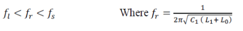
| The energy transfer capacitors C1 and C2 are important elements in the circuit since their values greatly influence the quality of input line current. Its values must be chosen such that their steady state voltages follow the shape of the rectified input ac line voltage waveform plus the output voltage with minimum switching voltage ripple as possible. Also, the values of C1 and C2 should not cause low frequency oscillations with the converter inductors. In practical design, values of C1 and C2 are determined based on inductors L1 , L0 values such that the resonant frequency(fr) during DCM stage is higher than line frequency(fl) and well below switching frequency(fs). Thus, | ||||||||||
 |
||||||||||
| Output capacitor C0 needs to be sufficiently large to store minimum energy required for balancing the difference between the time varying input power and constant load power. | ||||||||||
SIMULINK MODEL |
||||||||||
A. Simulink Models |
||||||||||
| The performance analysis of Controllable bridgeless CUK converter done by evaluating simulation waveforms. The tool used was MATLB SIMULINK. Fig. 6(a), 6(b), 6(c), 6(d) shows the simulation wave forms of input voltage and current, output voltage and input inductor current, gate signals to Q1 and Q2 respectively. | ||||||||||
| Simulation parameters are given below | ||||||||||
| a) Input Inductor : 25 mH | ||||||||||
| b) Output inductor : 1 μH | ||||||||||
| c) Output capacitance : 22000 μH | ||||||||||
| d) Energy transfer capacitor : 150 μF | ||||||||||
| e) Input voltage : 100 V AC | ||||||||||
B. Control Circuit |
||||||||||
| The feedback loop works with Sinusoidal Pulse Width Modulation (SPWM). Gate signals for Q1 and Q2 produced by the control circuit given in Fig. 5. Gate signals are proportional to the deviation of input current waveform from the desired shape. Input current wave form is compared with a desired sinusoidal signal. Difference of both signals (error signal) given as the input of PI (Proportional-Integral) controller. PI controller’s output compared with a triangular waveform of desired switching frequency. Output of relational operator provides the gate pulses. | ||||||||||
SIMULATION RESULTS |
||||||||||
| From simulation results we can understand that input current and voltage are in phase. So Power factor is nearly unity. Using this circuit we can improve the power factor up to 0.9136 with a power of 166 watts. | ||||||||||
COMPARISON STUDY |
||||||||||
| The Bridge less CUK converter circuit has higher component count, but lower current stresses [6][7]. The converter chooses according to the application. Efficiency of this circuit is higher than that of the conventional PFC CUK Rectifier for the provided output power levels due to lesser number of switches in conduction path. As the power level increases it shows some drawbacks. In this case, it is preferred to operate the converter in CCM region instead of DCM. Its THD value is less than 2%. For lower power levels they are designed to operate in DCM. DCM offers several advantages. With the introduction of closed loop control it become more stable with better Power Factor. Power factor improved from 0.9 to 0.916. Small and Simple control circuit is provided. | ||||||||||
CONCLUSION |
||||||||||
| Single –phase ac-dc bridgeless rectifier based on CUK topology are presented and discussed in this paper. The performance of the Bridgeless CUK converter topology is verified by simulation. Due to the lower conduction and switching losses, this topology can further improve the conversion efficiency compared to conventional system. To maintain the same efficiency, these circuits can operate with a higher switching frequency which helps to use small size filter components. It can possess low THD value less than 2%. It can work with near unity power factor. | ||||||||||
Figures at a glance |
||||||||||
|
||||||||||
References |
||||||||||
|


