Keywords
|
| DC power, dc-dc converter, Switching losses. |
INTRODUCTION
|
| IGBT is a voltage control device is used to convert one form of electrical power into other form by soft switching techniques. Among the other power semiconducting switches IGBT is the only device having property of transistor and MOSFET.[1] Additional auxiliary circuit is used for proper turn on and turn off of the dc to dc power converter. Low conduction losses are verified in the devices. |
| Where ever the low input voltage should be converted to high dc output voltage there dc chopping high power application circuit can be used. A step-up dc–dc converter which is the converter producing high dc voltage from low dc voltage are mainly used in industry especially as an interface circuit for batteries, solar cells, and more. Here the IGBT’s are used as switches in the inverting block instead of MOSFET’s in order to improve the efficiency of the circuit.[3] |
| The SCR, BJT, MOSFET and IGBT switches can be used. Here IGBT switch is used which is the combination of MOSFET and BJT in order to minimize the losses like switching and conduction losses. So IGBT produces the output with less losses that improves the efficiency of the circuit. |
RELATED WORK
|
| This dc to dc converter circuit consists of an input inductor named as Lin, the main switches S1–S4; the switches are IGBT switches, centre tapped transformer T with primary to each secondary turn’s ratio of 1: n and its leakage inductance of LL, rectifying diodes D1 and D2, and capacitor C, which is the converter output voltage filter. |
| The auxiliary circuit consists of auxiliary switch Sa, two auxiliary diodes Da1 and Da2, two coupled inductors La1 and La2 with turn’s ratio of 1: m, and the snubber capacitor of the main switches Ca. Current flowing through the switch is defined as drain to source current, and each switch voltage is drain to source voltage. |
PROPOSED SYSTEM
|
| Interval 1 starts by turning the auxiliary switch ON. By turning Sa ON, Ca voltage is present across La1 and its current increases in a resonance manner until Ca voltage decreases to V0/n.[5] Now the auxiliary switch turn on is under zero current (ZC) condition due to La1. |
| Interval 2, Da1 conducts and a resonance begins between LL, La1 and Ca. During this resonance, Ca voltage and LL current are decreasing, and La1 current increases. At the end of interval 2, LL current has reduced to zero and La1 current has increased to the sum of input current and Ca current. Assuming that I1 is much smaller than ILin |
| At interval 3, Ca completely discharges in a resonance with La1 |
| At interval 4 La1 current is greater than the input current. During this interval, energy is stored in the input inductor like when all the main switches are conducting. |
| The 5th interval starts by turning Sa OFF, and since Ca voltage is still zero, Sa turn off is under ZV condition. Because the total ampere turns off La1 and La2 should remain constant, Da2 conducts all the current and its current increases to I4/m. In this interval, S1– S4 are all conducting and they are equal, ie, IS1=IS2=IS3=IS4=(ILin+I4/m)/2 The next interval starts by turning S1 and S2 OFF and Ca is charged with current peak of I4/m + ILin At the interval 7, a resonance occurs between Ca and LL, and thus, Ca is charged to its peak value V1. The duration of this interval is small, La2 current can be assumed constant during this interval also. During the 8th interval, the voltage across La2 is essentially constant and equal to V0/n since LL value is much smaller than La2. |
| The 9th interval begins when La2 current has reached zero and Da2 turns off under ZC condition. In this interval, S3, S4 and D2 are conducting and the converter operates like a regular current-fed full-bridge converter. |
| A center tapped transformer is used in this project. A transformer is a static electromagnetic device used for the transformation of the alternating current from primary to secondary. The voltage can be controlled by changing the transformation ratio. This can be done by tapping the winding in order to alter the number of turns.[3] |
| The change in number of turns may be effected when the transformer is out of circuit or when on load. The tapping’s are provided on the high voltage winding because of a fine voltage variation is obtain owing to large number of turns. It is difficult to obtain voltage variation within close percentage limits in low voltage winding as there are few turns and voltage per turn is a large percentage of the total voltage.[6] |
| In transformer the tapping’s can be provided at, |
| (i) phase ends, and |
| (ii) neutral point or in the middle of the windings |
| When tapping’s are made at the neutral point the insulation between various parts are small. This arrangement is economical especially in the case of high voltage transformers. |
| These center tapped transformer are comes under the category of winding based classifications. In this it comes on sandwich coils. The advantage of this that their leakage can be easily controlled and so any desired value of leakage reactance can be had by the division of windings. |
| In the transformer side the voltage is conversion is, |
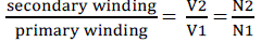 |
| Where, |
| V1 – primary voltage , V2 – secondary voltage |
| N1 – number of primary windings, N2 – number of secondary windings |
| The output voltage or the secondary voltage can be calculated by using the formula, |
Here, 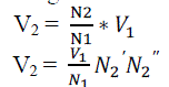 |
| For example, V1 = 50volts, N1 = 4, N2 = 4, N2 = 4 |
| Then the output voltage is V2 = 50*4*4/4 = 200volts |
EXPERIMENTAL SETUP
|
| The experiment model was done with MATLAB software. IGBT switches are used to convert DC power into AC power. Gate pulses also given to them. Diode are connected on the output side. A motor is additionlay connected with the output terminal to show the output voltage level through its working. Gate pulse and output speed of the motor are viewd by connecting scope of MATLAB. |
RESULT AND DISCUSSION
|
| The output voltage of the circuit is greater than the supply voltage. This is achieved by dc to dc converter circuit along with transformer circuit. Inversion dc to ac conversion and rectification dc to ac conversion process are done in the single circuit itself with low switching and conduction losses and low cost. Triggering pulses are given to the IGBT switches through PWM techniques. IGBT’s are turn on and turn off control switch which is just by giving and removing the pulses the IGBT device can be turned on and turned off. So the circuit doesn’t require additional circuit for turn off process like SCR.The ouput voltage obatined from MATLAB is shown. |
CONCLUSION
|
| In this project a small value of DC voltage is converted into a high value of DC voltage by using inverting and rectifying operations. Here the IGBT’s are used as switches in the inverting block instead of MOSFET’s and SCR’s. Among the power semiconductor switches IGBT is chosen here. The IGBT switches converted the high dc power with reduced conduction and switching losses. In this project MATLAB software is used for the simulation process. The related waveforms were shown. The circuit and simulated waveforms were shown by using MATLAB, and a separately excited DC motor is connected along with the circuit. The speed of the DC motor is monitored by the simulation block and controlled the converter technique. The low value of DC voltage is converted into high value of DC voltage by using this circuit and the less supply is utilized to run a dc motor which requires high dc voltage. |
Figures at a glance
|
 |
 |
| Figure 1 |
Figure 2 |
|
| |
References
|
- E. Adib and H. Farzanehfard, “Family of zero-current transition PWM converters,” IEEE Trans. Ind. Electron., vol. 55, no. 8, pp. 3055–3063 , Aug. 2008.
- E. Adib and H. Farzanehfard, “Family of isolated zero voltage transition PWM converters,” IET Power Electron., vol. 1, no. 1, pp. 144–153, 2008.
- C. M.Wang, C. H. Su, and K. L. Fang, “Zero-voltage-switching pulse width- modulation full-bridge transformer-isolated step-up/down converter,” IET Power Electron., vol. 1, no. 1, pp. 122–131 , 2008.
- C. M. Wang, “A novel ZCS-PWM flyback converter with a simple ZCS-PWM commutation cell,” IEEE Trans. Ind. Electron., vol. 55, no. 2, pp. 749–757, Aug. 2008
- Y. Gu, Z. Lu, Z. Qian, X. Gu, and L. Hang, “A novel ZVS resonant reset dual switch forward DC–DC converter,” IEEE Trans. Power Electron. , vol. 22, no. 1, pp. 96–103, Jan. 2007..
- Y. K. Lo and J. Y. Lin, “ Active clamping ZVS flyback converter employing two transformers,” IEEE Trans. Power Electron., vol. 22, no. 6, pp. 2416–2423 , Nov. 2007.
- N. Lakshminarasamma and V. Ramanarayanan, “A family of auxiliary switch ZVS-PWM DC-DC converters with coupled inductor ,” IEEE Trans. Power Electron., vol. 22, no. 5, pp. 2008–2017, Sep. 2007.
- P. Das and G. Moschopoulos, “A zero-current-transition converter with reduced auxiliary circuit losses,” IEEE Trans. Power Electron., vol. 22, no. 4, pp. 1464–1471, Jul. 2007.
- J. Zhang, X. Xie, X. Wu, G. Wu, and Z. Qian, “A novel zero current transition full bridge DC/DC converter,” IEEE Trans. Power Electron. , vol. 21, no. 2, pp. 354–360, Mar. 2006.
- L. Zhu, “A novel soft-commutating isolated boost full-bridge ZVS-PWM DC-DC converter for bidirectional high power applications,” IEEE Trans. Power Electron. , vol. 21, no. 2, pp. 422–429, Mar.2006.
- B. R. Lin and F. Y. Hsieh, “Soft switching zeta-flyback converter with a buck-boost type of active clamp,” IEEE Trans. Ind. Electron., vol. 54, no. 5, pp. 2813–2822, Oct. 2007.
- X. Wu, J. Zhang, X. Ye, and Z. Qian, “Analysis and design for a New ZVS DC–DC converter with active clamping ,” IEEE Trans. Power Electron., vol. 21, no. 6, pp. 1572–1579, Nov. 2006.
|