International Journal of Advanced Research in Electrical, Electronics and Instrumentation Engineering
ISSN ONLINE(2278-8875) PRINT (2320-3765)
ISSN ONLINE(2278-8875) PRINT (2320-3765)
Leena Thomas1, Midhun S2, Mini P K3, Josnie Ann Thomas4, Krishnapriya M N5
|
| Related article at Pubmed, Scholar Google |
Visit for more related articles at International Journal of Advanced Research in Electrical, Electronics and Instrumentation Engineering
The purpose of this project is to design and test a functional proof DC to DC boost converter. A microcontroller provides the necessary control signal to the switching circuit and it also monitors the input and output voltage levels. The input and output voltages are displayed on an LCD. Based on the input from a potentiometer, the microcontroller adjusts the duty cycle of the control signal thereby controlling the output voltage. An input voltage between 3-12 volts can be given and the device can produce a maximum voltage of 25V. This device is particularly useful in situations where standard voltage requirements do not match user’s application.
Keywords |
||||||||
| ATmega32A, buck boost converter, Schottky diode, power MOSFET | ||||||||
INTRODUCTION |
||||||||
| Power supplies are perhaps the most crucial elements of a battery-powered system. Battery-powered systems often stack cells in series to achieve higher voltages, but this is not always possible due to a lack of space. Switching converters use an inductor’s magnetic field to alternately store energy and release it to the load at a different voltage. With low losses they are a good choice for high efficiency. Capacitors connected to the converter’s output reduce output voltage ripple. A switching power supply consists of a power stage and a control circuit. The power stage performs the basic power conversion from the input voltage to the output voltage and includes switches and the output filter. The control circuit monitors the output voltage and controls the power switch. The control circuit comprises of a microcontroller which generates the necessary control signal to turn on the power switch. The duty cycle of the control signal is varied to adjust the output voltage. The output voltage is monitored by the in-built ADC unit of the microcontroller. | ||||||||
BASIC DC BOOST CONVERTER |
||||||||
| Boost converters are essentially a step-up converter that take in a low voltage input and provide an output at much higher voltage. The circuit diagram of the basic boost converter is shown in the figure below. | ||||||||
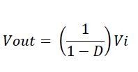
| The input and output voltage relationship is controlled by the duty cycle, D, of the switch according to the equation given below. | ||||||||
 |
||||||||
A. Selection of Components |
||||||||
| Inductor selection is a critical part of inductive-boost circuit design because the inductance value affects input and output ripple voltages and currents. An inductor with low series resistance provides optimal power conversion efficiency. In this paper, a 48μH toroidal inductor is chosen. The DC resistance of the inductor winding is 0.03Ω. | ||||||||
| A power MOSFET is used as the switch. The MOSFET is so chosen that its breakdown voltage is greater than the maximum output voltage of the converter and the on state voltage drop across it (RDS(ON)) is very small. Here, an Nchannel power MOSFET - IRFZ44 is used as the switch. It has a breakdown voltage of 60V and RDS(ON)=0.024Ω. | ||||||||
| Compared to a conventional diode, the Schottky diode provides a lower forward drop, yielding lower power dissipation and higher efficiency. The average current rating of the Schottky diode should be higher than the peak inductor current of the application. The reverse breakdown volt-age of the diode should be greater than the maximum output voltage of the circuit. Schottky diode 1N5822 is chosen. It has VRRM=40V and maximum value of average rectified forward current is 3A. | ||||||||
| Aluminum electrolytic capacitors are chosen for both input and output. For the input side, a 470μF, 25V capacitor is chosen and for the output side, a 330μF, 63V capacitor is chosen. | ||||||||
B. The Microcontroller |
||||||||
| The high-performance, low-power Atmel 8-bit AVR RISC-based microcontroller combines 32KB of programmable flash memory, 2KB SRAM, 1KB EEPROM, an 8-channel 10-bit A/D converter, and a JTAG interface for on-chip debugging. The device supports throughput of 16 MIPS at 16 MHz and operates between 4.5-5.5 volts. | ||||||||
| A 5 volt regulator circuit using the popular 3-terminal 7805 IC is used to supply the microcontroller and the LCD. 7805 is a linear voltage regulator that can output a maximum current of 1A. Capacitors are provided at both input and output side of the regulator to suppress noise. | ||||||||
| The Output Compare Unit of the 16-bit Timer1 of Atmgea32A is used for generating PWM signal. This signal is then given to the gate of the power MOSFET through a series resistor. The 16-bit Timer1 of Atmega32A works in fast PWM Mode. The fast Pulse Width Modulation or fast PWM mode provides a high frequency PWM waveform generation option. The fast PWM differs from other PWM options by its single-slope operation. The counter counts from BOTTOM to TOP and then restarts from BOTTOM. The TOP is specified by the value written to the Input Capture Register1 (ICR1). The compare value is written to the Output Compare Register A of Timer 1 (OCR1A). By varying the value of ICR1, the frequency of the PWM signal can be varies and by varying OCR1A, the dutycycle can be varied. | ||||||||
C. Voltage Monitoring and Display |
||||||||
| A resistive voltage divider circuit is used to reduce the DC input and output voltages to a maximum value of 2.5V. The resistors used are of ±1% tolerance. The input voltage is measured through pin ADC0 and the output voltage is measured through pin ADC1 of the Atmgea32A. The voltage measurement circuit also contains a multi-turn potentiometer for fine adjustment of voltage, a 4.7V zener diode for protection of ADC pins against overvoltage and a MOSFET to turn on the measurement circuit only when the voltage is to be read. Using a MOSFET in this way reduces the power loss in the resistor elements. | ||||||||
| The display used is a 16x2 character LCD display with HD44780U dot-matrix liquid crystal display driver and controller. The LCD is wired in 8-bit mode. The data pins of the LCD are connected to PORTC of ATmega32A and the RS, R/W and E pins of LCD are respectively connected to PB0, PB1 and PB2 pins of ATmega32A. | ||||||||
| The ATmega32A contains an internal 10-bit ADC. An internal 2.56V is used as the reference voltage for the ADC. The input and output voltages are read through channels ADC0 and ADC1 respectively. The value obtained is multiplied by suitable constants and is displayed on the LCD. The voltage measurement circuit should be calibrated first. This is done by applying a known value of input voltage and then adjusting the multi-turn potentiometer so that the voltage displayed on LCD is same as that of the input. Similar procedure is adopted for calibrating the output. The ADC2 pin of ATmega32A reads the input from a 10K potentiometer and based on this value the controller adjusts the dutycyle of the control signal. | ||||||||
CIRCUIT DIAGRAM |
||||||||
CONCLUSION |
||||||||
Accomplishments |
||||||||
| Overall, the main objective of this project was achieved. The boost converter, with an operating frequency of 200 KHz, provided output voltages exceeding 20V with inputs as low as 8V. The input and output voltage measuring circuits worked better than expected, with errors as low as ±0.1V.The microcontroller flawlessly displayed these values on the LCD screen. | ||||||||
Pit-falls and Possible Improvements |
||||||||
| The output voltage varies with variation in load. As load increases, the output voltage drops. This could be avoided by monitoring the output voltage and making suitable adjustments in the dutycycle of the control signal to keep the output voltage constant. | ||||||||
| There is no true shutdown of the boost converter. Even when the control signal is not given, the output voltage will be same as that of the input. This problem can be solved by providing a power switch in series with the Schottky diode. The output voltage will then be zero whenever the power switch is turned OFF. | ||||||||
Figures at a glance |
||||||||
|
||||||||
References |
||||||||
|


