International Journal of Advanced Research in Electrical, Electronics and Instrumentation Engineering
ISSN ONLINE(2278-8875) PRINT (2320-3765)
ISSN ONLINE(2278-8875) PRINT (2320-3765)
Pulla Sravani Kumari1, Kasthuri Gunavardhan2
|
| Related article at Pubmed, Scholar Google |
Visit for more related articles at International Journal of Advanced Research in Electrical, Electronics and Instrumentation Engineering
In this paper, the design methodologies are used to obtain the multiple outputs of DC-DC converter with a coupled inductor. The proposed system consists of single input of low voltage level, which can be boost into two different voltage levels. In this topology a coupled inductor with only one power switch is utilized for voltage clamping and soft switching operation. The two output voltages in this topology are obtained by limited components. The output voltages obtained are middle voltage and high voltage terminals are taken as power for a dc load applications. This topology is developed for high efficiency power conversion and two different voltages for dc loads. The proportionalintegral derivative (PID) controller is designed in DC-DC converter to reduce the rise time and steady state error, and is modelled using SIMULINK and simulation results are obtained. It is referred as single input multiple output DC-DC converter.
Keywords |
||||||||||
| Coupled inductor, high-efficiency power conversion, single-input multiple-output (SIMO) converter, soft switching, voltage clamping. | ||||||||||
INTRODUCTION |
||||||||||
| In recent years the demand of energy is growing, rising the public awareness for environment. To protect the earth from global warming, created demand for the development of clean energy without pollution, have resulted in much of the research work focused on clean energies, such as fuel cell (FC), photovoltaic, and wind energy, etc., Because of the electric characteristics of clean energy, the generated power is critically affected by the climate or slow the transient responses, and the output voltage by load variations are easily influenced [1]-[3]. To ensure the proper operation of clean energy, other auxiliary components, e.g., storage elements, control boards, etc., are usually required. The fuel cell generation is one of the most efficient solutions for environmental pollution. In general various DC-DC converters with different voltage gains are made to satisfy the requirement of different voltage levels, so that the system control is complicated and corresponding cost is more expensive [4]. Here the conventional SIMO DC-DC converter capable of generating buck, boosts, and inverted outputs simultaneously. However, over three switches for one output were required. This scheme is suitable for only the low output voltage and power application, and its power conversion is degenerated because of hard switching operation. | ||||||||||
| Although a multi-output DC-DC converter shared zero-current-switching (ZCS) lagging leg having soft switching property can reduce the switching losses, but it is a three full-bridge converter scheme of more complicated. By this scheme the high-efficiency power conversion is difficult to achieve, and its cost is more expensive [5]-[6]. This paper presents a newly designed SIMO converter with a coupled inductor and uses one power switch to achieve its objectives of high-efficiency power conversion, high step-up ratio, and different and different voltage levels. In SIMO converter the utilisation of a low-voltage-rated power switch with small RDS (on), the soft switching techniques and voltage clamping are obtained to reduce the switching losses. The slew rate in the coupled inductor causes change in current it is restricted by leakage inductor [7]. The current transition time enables the power switch to turn ON with property of ZCS easily, and the effect of the leakage inductor can make less severe the losses caused by the reverse recovery current. The voltages of middle-voltage output terminals can be approximately adjusted by the design of auxiliary inductors and the high voltage DC bus can be stably controlled by a voltage proportional-integral derivative (PID) control. The section VI provides results to validate the effectiveness of the proposed SIMO converter and conclusions are drawn in section V. | ||||||||||
CONVERTER DESIGN AND ANALYSIS |
||||||||||
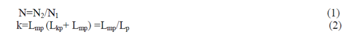
| The proposed system consists of high-efficiency SIMO converter topology to generate two different voltage levels from a single-input power source is depicted in Fig. 1. This SIMO converter contains five parts in this topology a lowvoltage- sides circuit (LVSC), a clamped circuit, a middle-voltage circuit, an auxiliary circuit, and a high-voltage-side circuit (HVSC). The major symbol representations are VFC (iFC) and VO1 (iO1) denote the voltages (currents) of the input power source and the output load at the LVSC and the auxiliary circuit, respectively; VO2 and iO2 are the output voltages and current in the HVSC whereas CFC, CO1, and CO2 are the filter capacitors at the LVSC is the auxiliary circuit, and the HVSC, respectively; C1 and C2 are the clamped and middle-voltage capacitors in the clamped and middle-voltage circuits, respectively, Lp and Ls represent individual inductors in the primary and secondary sides of the coupled inductor Tr, respectively, where the primary side in connected to the input power source Laux is the auxiliary circuit inductor. The main switch is expressed as S1 in the LVSC; the equivalent load in the auxiliary circuit is represented as RO1 and the output load is represented as RO2 in the HVSC. The corresponding equivalent circuits is given in Fig. B is used to define the voltage polarities and current directions. The coupled inductor in Fig. A can be modelled as an ideal transformer including the magnetizing inductor Lmp and the leakage inductor Lkp in Fig. B. The turns ratio N and coupling coefficient k of Fig. B Equivalent circuit. This ideal transformer defined as | ||||||||||
 |
||||||||||
| where N1 and N2 are the winding turns in the primary and secondary sides of the coupled inductor Tr. Because the voltage gain is less sensitive to the coupling coefficient and the clamped capacitor C1 is approximately selected to completely absorb the leakage inductor energy, the coupling coefficient could be simply set at one (k=1) to obtain Lmp= LP via (2). In this study, the following assumptions are made to simplify the converter analyses: The main switch including its body diode is assumed as an ideal switching element; and the conduction voltage drops of both the switch and diode are neglected. | ||||||||||
OPERATION MODES |
||||||||||
| The characteristics waveforms are shown Fig. C and the topological modes in one switching cycles are illustrated in Fig.4. | ||||||||||
| Mode 1(t0âÃâÃâ¬t1) [Fig (a)]: In this mode, the main switch S1 was Turned ON for a span, and the diode D4 Turned OFF. Because the polarity of the winding of the coupled inductor Tr is positive, the diode D3 turns ON. The secondary Current iLS reverses and charges to the middle voltage capacitor C2.When auxiliary inductor Laux releases its stored energy completely, and the diode D2 Turns off, this mode ends. | ||||||||||
| Mode 2 (t1−t2) [Fig (b)]: At time t =t1, the main switch S1 is persistently turned ON. Because the primary inductor LP is charged by input power source, the magnetizing current iLmp increases gradually in an approximately linear way. At the same time, the secondary voltage VLS charges the middle-voltage capacitor C2 through the diode D3.Athough the voltage VLmp is equal to the input voltage VFC both at modes 1and 2, the ascendant slope of the leakage current of the coupled inductor (diLkp/dt) at modes1 and2 is different due to path of the auxiliary circuit. Because the auxiliary inductor Laux releases its stored energy completely, and the diode turns OFF at the end of mode 1, it results in reduction of diLkp/dt at mode 2. | ||||||||||
| Mode 3 (t2âÃâÃâ¬t) [Fig (c)]: At time t= t2, the main switch S1 is turned OFF. When the leakage energy still releas2ed from the secondary side of the coupled inductor, the diode D3 persistently conducts and releases the leakage energy to the middle–voltage capacitor C2. When the voltage across the main switch VS1 is higher than voltage across the clamped capacitor VC1, the diode D1 conducts to transmit the energy of the primary –side leakage inductor Lkp into the Clamped capacitor C1.At the same time, partial energy of the primary-side leakage inductor Lkp is transmitted to the auxiliary inductor Laux, and the diode D2 conducts. Thus, the current iLaux passes through the diode D2 to supply the Power for the output load in the auxiliary circuit. When the secondary side of the coupled inductor releases its leakage energy completely, and diode turns OFF, this mode ends. | ||||||||||
| Mode 4(t3âÃâÃâ¬t4) [Fig (d)]: At the time t=t3, the main switch S1 is persistently Turned OFF. When the leakage energy has released from the primary side of the coupled inductor, the secondary current iLS is induced in reverse from the energy of magnetizing inductor Lmp through the ideal transformer, and flows through the diode D4 to the HVSC. At the same time, partial energy of the primary side leakage inductor Lkp is still persistently transmitted to auxiliary inductor Laux, and the diode D2 keeps conducting. Moreover, the current iLaux passes through diode D2 to supply the power for the output load in auxiliary circuit. | ||||||||||
| Mode 5 (t4âÃâÃ⬠t5) [Fig (e)]: At time t=t4, the main switch S1 is persistently turned OFF, and the clamped diode D1 Turns OFF because the primary leakage current iLkp equals to auxiliary inductor current iLaux. In this mode, the input power source, and the primary winding of the inductor Tr, and the auxiliary inductor Laux connect in series to supply the power for the output load in the auxiliary circuit through the diode D2, At the same time, winding of the input power source, the secondary coupled inductor Tr, the clamped capacitor C1, and the middle-voltage capacitor (C2) connect in series to release the energy into the HVSC through the diode D4. | ||||||||||
| Mode 6(t5âÃâÃâ¬t6) [Fig (f)]: At time t=t5, this mode begins when the main switch S1 is triggered. The auxiliary inductor Current iLaux needs time to decay to zero, the diode D2 persistently conducts. In this mode, the input power source, the clamped capacitor C1, the secondary winding of the coupled inductor Tr, and the middle-voltage capacitor C2 still connect in series to release the energy into the HVSC through the diode D4. Since the clamped diode D1 can be selected as a low –voltage Schottky diode, it will be cut off promptly without a reverse current. Moreover, the rising rate of the primary current iLkp is limited by primary-side leakage inductor Lkp. Thus, one cannot derive any currents from the paths of the HVSC, the middle-voltage circuit, the auxiliary circuit, and the clamped circuit. As a result, the main switch | ||||||||||
| S1 is turned ON under the condition of ZCS and this soft-switching property is helpful for alleviating the switching loss. When the secondary current iLS decays to zero, this mode ends. After that, it begins the next switching cycle and repeats the operation in mode 1. | ||||||||||
Voltage Gain Derivation: |
||||||||||
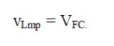
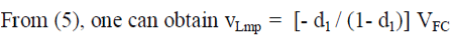
| Here the magnetising inductor voltage vLmp is equal to the input power source VFC at the mode 2, the voltage vLmp can be represented as | ||||||||||
 |
||||||||||
 |
||||||||||
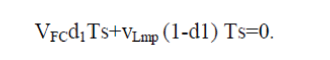
| By using the voltage-second balance, the relation of the average voltage across the magnetising inductor Lmp of coupled inductor Tr to be zero can be represented as | ||||||||||
 |
||||||||||
 |
||||||||||
| Since the voltage of the clamped capacitor VC1 is equal to the negative voltage of magnetising inductors voltage vLmp at modes 3 and 4, the voltage VC1 can be expressed as (6) | ||||||||||
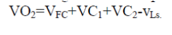
| According to Kirchhoff’s voltage law, the output voltage VO2 can be obtained as | ||||||||||
 |
||||||||||
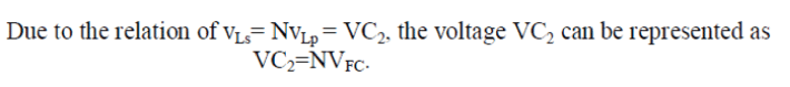
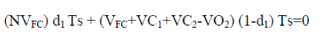
| By using the voltage-second balance, the relation of the average voltage across the secondary winding vLs to be zero, can be expressed by (4) and (8) as | ||||||||||
 |
||||||||||
| From (4)-(9), the voltage gain GVH of the proposed SIMO converter from the LVSV to the HVSC can be given as | ||||||||||
| For calculating the discharge time of the auxiliary inductor at modes 1 and 6, the corresponding time interval can be denoted as dx Ts = [(t6-t5) + (t1-t0)]. By using the voltage-second balance, the relation of the average voltage across the auxiliary inductor Laux to be zero can represented as | ||||||||||
| The voltage gain GVL of the proposed SIMO converter from the LVSC to the auxiliary circuit can be obtained by (6) and (11) as | ||||||||||
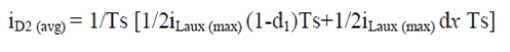
| Because the diode current iD2 is equal to the current iLaux, the average value of the diode current iD2 can be calculated. | ||||||||||
 |
||||||||||
| Where Ts is the converter switching cycle, iLaux (max) is the maximum current of the auxiliary inductor and can be expressed as | ||||||||||
| By substituting (14) into (13), one can obtain | ||||||||||
| Because the average current of the diode D2 is equal to the current iO1, it yields | ||||||||||
| From (15) and (16), the duty cycle dx can be rewritten as | ||||||||||
| By substituting (17) into (12), the voltage gain GVL of the proposed SIMO converter from the LVSC to the auxiliary circuit can be rearranged as | ||||||||||
SIMULATION RESULTS |
||||||||||
| Here, the proposed converter can boost the 12volts of a low-voltage input power source to a controllable high-voltage 200volts dc bus and middle-voltage output 28volts terminals. The high-voltage dc bus can take as the main power for a high-voltage dc load or the front terminal of a dc–ac inverter. Moreover, middle-voltage output terminals can supply powers for individual middle-voltage dc loads or for charging auxiliary power sources (e.g., battery modules). | ||||||||||
1. OPEN LOOP |
||||||||||
| The output voltages by above simulated circuit with single input of low voltage of 12V are obtained, two voltages of different levels as shown below. These voltages are obtained by the open loop circuit of SIMO converter shown below. | ||||||||||
2. CLOSED LOOP |
||||||||||
| The above simulation cicuit is closed loop topology of SIMO converter, Here the input voltage is 12V and output voltages are of two difrerent levels are 200V and 28V obtained. Here PID controller is suggested to reduce the output voltage variations. | ||||||||||
CONCLUSION |
||||||||||
| This paper has presented high-efficiency dc-dc converter, and this coupled-inductor-based converter was applied well to a single-input power source having two output terminals of an auxiliary battery module and a high-voltage dc bus. The results of SIMO converter is the maximum efficiency was measured to be exceed 95%, and the average conversion efficiency was measured over 91%.The proposed SIMO converter is suitable for the application such as one common ground, is preferred in most applications. The major scientific contributions of the SIMO converter are recited as follows: | ||||||||||
| 1) This topology has only one power switch to achieve the objective of SIMO power conversion. | ||||||||||
| 2) The voltage gain is substantially increased by using a coupled inductor | ||||||||||
| 3) The stray energy is recycled by a clamped capacitor into the auxiliary battery module or high-voltage dc bus to ensure the property of voltage clamping. | ||||||||||
| 4) An auxiliary inductor is providing the charge power to the auxiliary battery module and assisting the turned ON under the conditions of ZCS. | ||||||||||
| 5) The switch voltage stress is not on the input voltage so that it is more suitable for a dc conversion mechanism with different input voltage levels. | ||||||||||
| 6) The copper loss in the magnetic core can be greatly reduced, due to copper film with lower turns. | ||||||||||
Figures at a glance |
||||||||||
|
||||||||||
|
||||||||||
References |
||||||||||
|


