International Journal of Advanced Research in Electrical, Electronics and Instrumentation Engineering
ISSN ONLINE(2278-8875) PRINT (2320-3765)
ISSN ONLINE(2278-8875) PRINT (2320-3765)
Rosemary Mathai1, Bindu Elias2, Beena M Varghese3
|
| Related article at Pubmed, Scholar Google |
Visit for more related articles at International Journal of Advanced Research in Electrical, Electronics and Instrumentation Engineering
Conventional DC-DC converters are unable to provide high step up voltage gain due to reverse recovery problem of diodes. In this paper, DC-DC converter using switched inductor technique with feedback control is introduced to achieve high voltage gain without high duty ratio. In the DC-DC converter using switched inductor technique, two inductors with same level of inductance are charged in parallel during the switch on period and are discharged in series during the switch off period. Simulation has been carried out to study the performance of the converter. Further performance comparison of this converter is done with transformer less high step up DC-DC converter.
Keywords |
| switched inductor, cascode technique |
INTRODUCTION |
| Nowadays, high step up DC-DC converters are used in many applications such as renewable energy conversion. In order to achieve high voltage gain, the conventional boost converter must be operated at extremely high duty ratio [2]- [4]. However, due to the impacts of the reverse- recovery problem of the diodes, the conventional boost converter cannot achieve high voltage gain. |
| transformer less high step up DC-DC converter using cascode technique [1] is shown in figure 1. It consist of one switch S, three diodes D1, D01, D02, two inductors L1, L2 and output capacitors C01 and C02. Two buck boost convertersare integrated with the help of a single switch. There are four modes of operation for this circuit. |
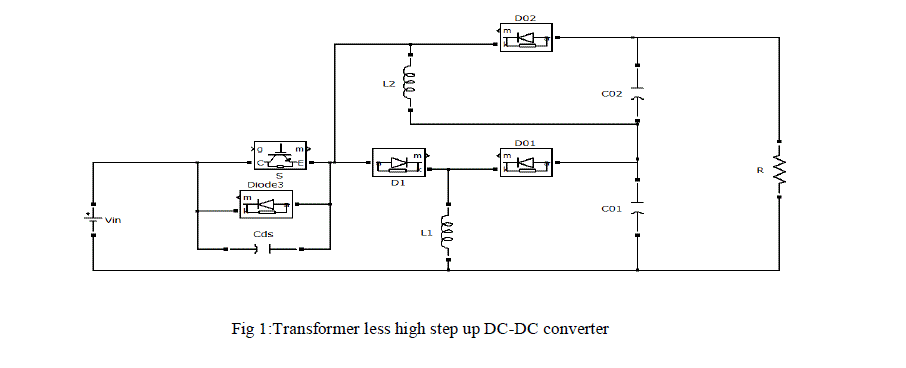 |
| In mode1, switch S is turned on. The energy is transferred from DC source to inductor L1 through switch S and diode D1. Also the DC source and capacitor C01 are series to release their energies to inductor L2 through switch S. In mode2, switch S is turned off. The energies stored in capacitorsC01and C02 are discharged to the load by series. The voltage across capacitor Cdsis charged to Vin+VCO1. In mode3, since the voltage across capacitor Cds is equal to Vin+VCO1, diode D01 is ON. The energy stored in inductor L2 is still released to capacitor Cds. The energy stored in inductor L1 is released to capacitor C01 and the load. In mode4, since the voltage across the capacitor Cds is equal to Vin+V0, diodes D01 and D02 are ON. The energy stored in inductors L1 and L2 are released to capacitors C01, C02 and load. Here high step up voltage gain can be achieved but voltage stress across the switch is high, since only one switch is there. The voltage stress on the switch equals the output voltage. Also polarity of output voltage is opposite to that of input voltage. |
| In this paper, DC-DC converter using switched inductor technique with feedback control is introduced with low duty cycle. In the proposed converter, two switches are included, thus the voltage stresses on the active switches are less than the output voltage. Also total harmonic distortion is reduced with the help of feedback control. The circuit analysis of the proposed converter is discussed in the following section. |
DC-DC CONVERTER USING SWITCHED INDUCTOR TECHNIQUE |
| A transformer less high step up DC-DC converter using switched inductor technique [5] is studied in this paper. The converter is shown in figure 2. It consists of two switches S1 and S2, two inductors L1 and L2with same level of inductance, one output diode D0 and one output capacitor C. There are two modes of operation for the circuit. In mode1, two switches are simultaneously turned on. Inductors L1 and L2 are charged in parallel from the DC source and the energy stored in output capacitor C is released to the load. Thus the voltage across L1 and L2 is equal to the input voltage. In mode2, two switches are turned off. The DC source, L1 and L2 are series connected to transfer the energies to capacitor C and load. |
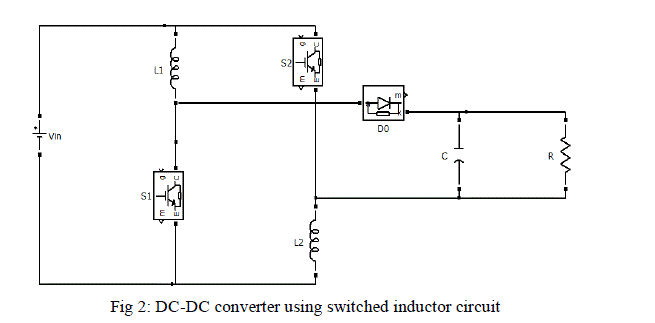 |
| In this converter, high step up voltage gain is achieved with low duty ratio. Voltage gain is the ratio of output voltage by input voltage. Here the voltage gain achieved is approximately 8. The voltage stress is the amount of voltage which appears across the switches. As the number of switches is two, voltage stress is greatly reduced and is equal to input voltage. |
FEEDBACK CONTROL |
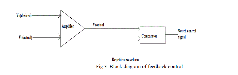
| Feedback control is provided to control the output voltage to the desired level. The block diagram of feedback control is shown in figure 3. In a dc-dc converter with a given input voltage the average output voltage is controlled by adjusting the switch on and off durations. The control voltage is generally obtained by amplifying the error signal or difference between actual voltage and desired voltage. Any change in the input voltage is sensed as change in output voltage and accordingly the error signal also changes. The error signal is used to change the duty ratio of the switching pulses to keep the voltage constant. |
 |
| The advantages of PWM technique are |
| 1. The output voltage control can be obtained without any additional components. |
| 2. Lower order harmonics can be eliminated or minimized along with its output voltage control. As higher order harmonics can be filtered easily, the filtering requirements are minimized. |
SIMULATION RESULTS |
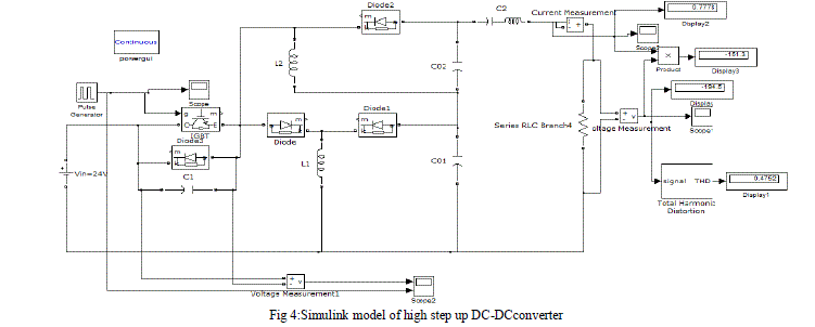
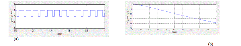
| The simulation of transformer less high step up DC-DC converter, DC-DC converter using switched inductor technique with and without feedback has been done in MATLAB/SIMULINK. The switching frequency is taken as 50Hz.The simulink model of high step up DC-DC converter is shown in fig 4. The circuit parameters of transformer less DC-DC converter are selected as input voltage Vin =24V, capacitors C01=0.01F, C02= 0.5F, C1=1μF and inductors L1= L2=1mF.Duty cycle of the switch is taken as 70%. The simulation results of gate pulse to switch S, capacitor voltage, output voltage and output current are shown in figs 5(a), 5(b), 5(c), 5(d) and 5(e) respectively. Output voltage of transformer less DC-DC converter is -194.5V. |
 |
 |
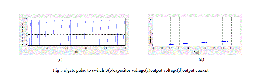 |
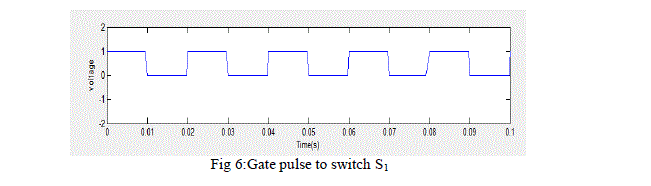
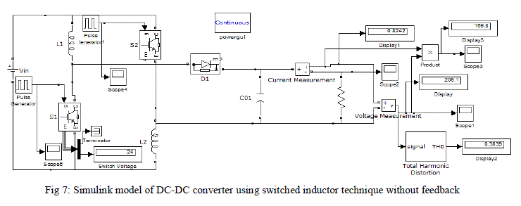
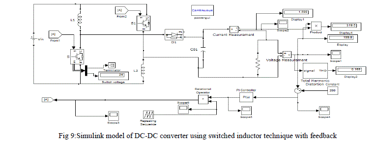
| From the above simulation results it is clear that, when switch is turned off, capacitor is charging and voltage stress across switch is 225V. Also the output voltage is opposite to that of input voltage since we are using two buck boost converters.The Simulink model of DC-DC converter using switched inductor technique with and without feedback are shown in fig 7 and 9 respectively. The circuit parameters of both circuits are selected as input voltage Vin=24V, inductors L1=L2=1mH, capacitor C01=0.21F. The switches S1 and S2 are given the same control signal. The duty cycle of the switch is taken as 50%. Gate signals for the switch S1, simulated waveforms of output current and output voltage are shown in fig 6, 8(a) and 8(b) respectively. Output voltage of switched inductor circuit is 206.1V. |
 |
 |
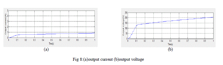 |
| From the simulation results, it is clear that, the voltage stress across the switch is reduced to 24V. Also, it can be seen that the polarity of output voltage is same. |
 |
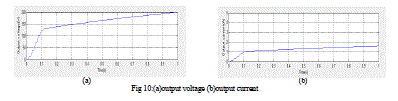 |
| From the simulation results, it is clear that, the voltage stress across the switch is 24V. Also, total harmonic distortion is reduced to 16.5% with the help of feedback. Simulation results are summarized in the table shown. |
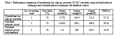 |
| The simulation results are analysed and the comparison of %THD with and without feedback is studied. Table 1 shows the comparison of three types of DC-DC converters. It can be summarized that, the proposed converter has the following merits: |
| 1. Step up voltage gain in the range of 8 can be achieved. |
| 2. High step up voltage gain is achieved with 50% duty cycle. |
| 3. Voltage stress across the switch is reduced as the number of switches is two. |
| 4. Total Harmonic distortion is reduced to 16.5% with the help of feedback. |
CONCLUSION |
| In this paper, DC-DC converter using switched inductor technique with feedback control is introduced. With this converter, high step up voltage gain is achieved with low duty ratio. The converter is analyzed and simulation results are presented. Then the performance comparison of converter is done with the transformer less step up converter and DC-DC converter with switched inductor technique. From simulation results, it is clear that when transformer less step up converter is used voltage stress across the switch is 225V and when switched inductor circuit is used, the voltage stress across the switch is reduced to 24V. That is with the help of switched inductor circuit, voltage stress is reduced to 1/9 times. It can be concluded that, the DC-DC converter using switched inductor technique with feedback control have total harmonic distortion reduced to 16.5% and duty ratio 50% with output voltage 220V. |
References |
|