International Journal of Advanced Research in Electrical, Electronics and Instrumentation Engineering
ISSN ONLINE(2278-8875) PRINT (2320-3765)
ISSN ONLINE(2278-8875) PRINT (2320-3765)
LI Nan1, DENG Gang2, KONG Bing2
|
| Related article at Pubmed, Scholar Google |
Visit for more related articles at International Journal of Advanced Research in Electrical, Electronics and Instrumentation Engineering
The 35 kV prefabricated silicone rubber cable terminal defect models were established and simulated in the static electric field utilizing the finite element method. Triangle and isosceles trapezoid models were established to simulate the incised defects and sunken defects where partial discharge might occur. Defects with different sizes and same length-width ratio were built to calculate the maximum field strength. The distribution of maximum field strength was drawn into curves with the least square interpolation data. The results indicate that the fracture of the copper shield is easy to cause electric field distortion and partial discharge. The electric field strength of incised defect is higher than that of the sunken one in the same place. Due to the evacuated effect of the stress cone, it is less likely to cause partial discharge in the fracture of semi-conducting layer. It may cause partial discharge in the long run if there is micro air gap in area between the fracture of copper shield and semi-conducting layer. The conclusions have certain guidance on the design, manufacture and installation of cable terminal.
Keywords |
||||||||||
| cable accessory; partial discharge; finite element method; micro gap. | ||||||||||
INTRODUCTION |
||||||||||
| It is easy to cause partial discharge of cable terminal due to the striping of semi-conducting layer and the copper shield which leads to local electric field distortion. In order to improve the local field intensity concentration, the stress control tube is often used to evacuate stress and reduce the local field strength. It often causes defects, such as semiconducting layer insulation incising, stress cone shifting and micro-gaps with gas or small impurities during the cable terminals installation, which may cause partial discharge and lead to breakdown after a long run [1]. A large amount of data shows that the partial discharge is one of the main reasons for cable insulation damage and the cable accessories are one of the weakest sections. Therefore, research on cable accessories defect model of partial discharge is of great significance. The domestic and overseas researches on cable terminal include the aspects of sensors and detection method [2], mathematical modeling and simulation [3, 4], fault diagnosis and identification of partial discharge data [5] and partial discharge experiments [6-9]. The current main methods of signal processing include wavelet analysis and its derivative algorithm, the K-means clustering algorithm, pattern recognition method, support vector machine (SVM) theory, fractal, Wei-bull transformation, etc. | ||||||||||
| Currently, the researches on the relation of the partial discharge degree and the gap sizes are rare. Using blade electrodes, T. Asokan has done some research on the electrical discharge characteristics of micro-gaps [10], which ranges from 50μm to 1000μm in air. The study shows that the micro gaps less than 1000 microns no longer meet the Paschen's law, and with the gap decreasing, the field intensity shows an increasing trend. The air gap between the electrodes has been studied, however, the actual cable accessories or other power equipments have not been considered. H. Illias developed a simulation model for spherical cavities within a homogeneous dielectric material [11], and the model was implemented using the Finite Element Analysis (FEA) software. Electric field distributing and discharging characteristics can be obtained by studying on spherical cavity with different diameters and locations. Due to the complexity of the shape and the internal characteristics of actual cable accessories, in addition with the effect of stress cone and copper shield, it is necessary to do some research on the relationships between internal defect morphological characteristics of cable accessory and partial discharge. Reference [6] simulated and tested the electric field distributing under the defects of axial air gap with different width in the main insulation of 10kV cable terminal. Reference [7] simulated the air gap defect partial discharge at the point of the Semi-conducting layer of 220 kV cable joints. These simulations or tests just aim at one kind of air gap defects that may occur instead of considering all kinds of defects according to the reality, which is the key point of this article. | ||||||||||
| In view of different kinds of common defects at the high voltage cable terminals, this article has simulated micro gap defect models [12-14] with different sizes and shapes using the finite element simulation software based on 35 kV cable termination physical objects with consideration of the effect of stress cone and copper shield. Curves of maximum field strength changing with different defect sizes have been achieved by fitting the experimental data with the least square method. | ||||||||||
SIMULATION OF ELECTROSTATIC FIELD BASED ON THE FINITE ELEMENT ANALYSIS |
||||||||||
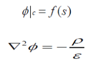
| The finite element method is a numerical calculation method based on variation principle and subdivision interpolation [15]. First of all, the boundary value problem needed to solve is transformed into the corresponding variational problem using the variation principle, the so-called functional extremum problem. Then the variation problem is discretized into a general multivariate function extremum problem through subdivision interpolation. Ultimately comes down to a set of algebraic equations and the numerical solution of boundary value problem can be obtained by solving it. In the plane domain D, the boundary is c, electric charge density is ρ, permittivity is ε and the electric potential is φ. They meet the first kind of boundary value conditions and Poisson equation under the condition of two-dimensional electrostatic field [16].That is | ||||||||||
| and | ||||||||||
 |
||||||||||
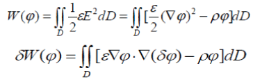
| The function of electric field energy is shown in equation (1). Well, the variation is shown in the following equation (2). | ||||||||||
 |
||||||||||
| The condition of minimum energy of the electric field is described as follows: | ||||||||||
| Where, δ is the variational symbol, E is the field intensity for the unit, âÃâý is the Hamiltonian operator and D is the integral area. | ||||||||||
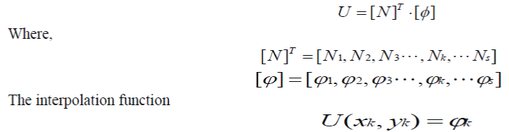
| Considering the known boundary potentials, equation (3) will not be considered. Subdivide domain D into a finite number of discrete polygon sub-domains (triangular or quadrilateral), the function ÃÂä within each unit can be approximated by a appropriate interpolation function U (x, y) [17]. Suppose that U is represented by shape function matrix of coordinates and the node potential function matrix, that is | ||||||||||
 |
||||||||||
| Through simultaneous equations (4), (5) and (6), the interpolation numerical solution of the problem can be worked out. Field size and electric energy of each sub-domain can be calculated by equation (1) with the calculated potential distribution. | ||||||||||
MODEL ANALYSIS AND ESTABLISHED |
||||||||||
| In this paper, ANSYS finite element two-dimensional model is established according to the proportion of 1:1 based on the design drawing of 35 kV cable termination (fig 1).The real terminal is shown in fig 2. | ||||||||||
| Two kinds of defects with different sizes and shapes have been established to simulate the incision and sinking, where the partial discharge may occur, such as the fractures of conductive layerïüÃÅthe fractures of copper shield and the conductive layer areas between the these two fractures. One of those defect models is shown in fig 3. The figure is pictured as silicone rubber coat, stress cone, a conductive layer, cable main insulation, cable inner semi-conducting layer and the cable core from top to bottom respectively. The incise defect is simulated by triangle, and the sunken defect is simulated by isosceles trapezoid at semi-conducting layers and copper shield fractures. Two kinds of defects have been simulated by triangle at conductive layer fractures. | ||||||||||
| Potential distribution and the electric field intensity vector sum can be acquired by simulation of electrostatic field model using finite element method. Defect models at different positions are listed in tab 1. | ||||||||||
| Instruction: âÃâàand âÃâã locate in the copper shield fracture inside the semi-conducting layer; âÃâá andâÃâä locate between two fractures inside the Semi-conducting layer; âÃââ locates in semi-conducting layer fracture inside major insulation; âÃâÃÂ¥ locates in semi-conducting layer fracture inside the stress cone. | ||||||||||
| Defect models with same proportion and different sizes have been established for simulation and verification in the above table. The defects occur in the cable terminal may have different types such as surface discharge, conductive particle discharge, inner air gap discharge and cable burr discharge. These defects are eventually due to micro gaps filling with air or other impurities. Those defects have different permittivities with the surrounding insulations (in most cases, the permittivity is lower), so as to cause the concentration of electric field distribution. Therefore, all the defects may occur in cable terminal can be simulated by the incise defect and the sunken defect with different permittivities. Permittivity and conductivity of different materials in 35 kV cable terminals can be seen in tab 2. During simulation test, 35kV voltage is applied at the cable core and 0 kV voltage is applied at external surface of the terminal and copper shield. When meshing the models, the unified division with smart size of 4 is adopted and the level 5(maximum) refinement is applied when refining. | ||||||||||
FITTING BY THE LESAT SQUARE METHOD AND ANALYSIS OF EXPERIMENTAL RESULTS |
||||||||||
4.1 Fitting by the least square method |
||||||||||
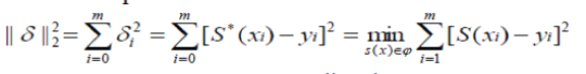
| On the premise of error minimization, the least square method can fit discrete data into linear function (the smooth curve) according to a certain standard. It can be intuitively expressed by mathematical expression and the results can be used for further experimental data analysis. For a set of given data (xi, yi)(i = 0,1,,m) , a function y =S (x) can be found in function class, where the error sum of squares meets: | ||||||||||
 |
||||||||||
| In which | ||||||||||
| When fitting curve by the least-square method, the type of S (x) must be determined firstly which is related to variation tendency of data. Rules discussed in this paper are the relationships between the maximum field strength and the size of the infect models. Singular points do not conform to the laws will be ignored by the least square method and a smooth curve will pass through a set of two dimensional points, so fitting data by this method can response the change rule of the research question preferably. Mathematical statistics gathers the maximum field strength of defect models with different sizes after simulation and then the data is fitted by the least square method. | ||||||||||
| Steps of fitting: | ||||||||||
| 1) Select the interpolation function and times to be fit according to the data characteristics. | ||||||||||
| 2) Calculate the coefficient of the fitting function according to the curve fitting rule of the least squares. | ||||||||||
| 3) Fit and plot. | ||||||||||
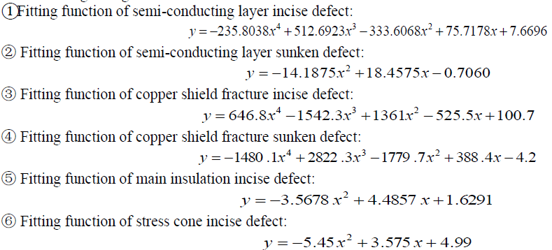
| The following fitting functions have been obtained: | ||||||||||
 |
||||||||||
4.2 Analysis of experimental results |
||||||||||
| Previous studies often ignore the existence of copper shield when simulation. However, the copper shield is of crucial significance and the weak link to cause partial discharge. The copper shield acts as a channel for capacitance current flowing through under normal circumstances and for short-circuit current flowing through while there is a short circuit [18]. At the same time, it also has the effect of shielding electric field. Due to the existence of micro gap defects, the value of contact resistance increases and the short circuit capacity is limited. In addition, the current does not flow along the axial direction but around the axis of spiral, and it causes the inductance which will increase the induced electromotive force. As shown in fig 4 (a), when the defect exists at the copper shield fracture, the field strength increases dramatically and the average field intensity is greater than that of the air breakdown (30 kV/cm). Among them, the field strength of incise defect decreases as the size increases and the maximum field strength is close to 100 kV/mm which is easy to cause the increased aging of insulation materials and the partial discharge when the size of gap is less than 0.1 mm. As a result, the copper shield fracture is more likely to become the origin of the partial discharge. So the DC resistance, induced voltage and induced current should be tested conscientiously. Replace the aging terminal in time, which helps to avoid the happening of the accidents. | ||||||||||
| In the simulation of ignoring the copper shield at the semi-conducting layer fracture, incise defect inside major insulation causes a large field strength which causes partial discharge easily. When considering the copper shield, the problems of large field strength are improved due to the shielding effect of the copper shield to electric field and the evacuating effect of stress cone. As shown in fig 4 (b), the average field intensity is controlled under 4.5 kV/mm. Because the semi-conducting layer and the stress cone have good contact and similar permittivity, they can be seen as a whole when calculating by finite element method. Cable main insulation has a smaller permittivity than semiconducting layer and stress cone which is close to the permittivity of air. As a result, this kind of defects is less likely to cause partial discharge than what has previously introduced. | ||||||||||
| The electric field stress concentrates near the copper shield fracture because of the removal of copper shield, and the electric field stress of areas between the copper shield fracture and semi-conducting layer fracture also changes. As shown in fig 4 (c), the electric strength of incise defect is higher than that of the sunken defect and is proportional to the depth of incising. The average field intensity is larger than 10kV/mm which exceeds the maximum field strength of air breakdown. The permittivity around the defect areas will decrease in long run. Because there is inverse proportional relationship between field strength and permittivity and the defect has lower permittivity, the higher electric strength occurs in defect, reinforcing a vicious cycle. Thus, it speeds up the aging and eventually causes partial discharge. | ||||||||||
| According to the simulation results of various types of cable terminal defects, the maximum field strengths of defects are obtained. Possibilities of discharge for all kinds of defects are forecast in tab 3. | ||||||||||
| The experimental data shows that the maximum electric strength of incise defect is higher than that of the sunken defect where it probably causes partial discharge. The sharper the able terminal defect model, the more seriously distorted the electric field, and this is consistent with the predecessors' research results. | ||||||||||
EXPERIMENTAL VERIFICATION |
||||||||||
| The anatomy of the physical objects of 35 kV XLPE cable terminal replaced from field is consistent with the simulation conclusion. When checking the fault cable terminal, the micro air gap is found in copper shield fracture (which has not been polished so as to create a micro air gap). On the other hand, the semi-conducting layer fracture is sunken, which contributes to create a step air gap defect. At last, the stress control glue has daubed uneven at the end of copper shield. As shown in fig 5, the discharge position locates at the end of copper shield (within the scope of the red circle). | ||||||||||
CONCLUSION |
||||||||||
| Incise defects and sunken defects of the 35 kV cable terminals with different sizes and shapes are simulated utilizing the finite element method, and the maximum field strength distribution is obtained. Fitting the data with the least square method and the following conclusions are reached through the simulations and demonstration analysis: | ||||||||||
| 1) The closer to the copper shield fracture, the weaker the stress control, and the greater the local field strength. | ||||||||||
| 2) The incise defects is more likely to cause partial discharge than the sunken ones because of higher electric strength with the same size at the same position. | ||||||||||
| 3) There are stress concentration and the higher field strength at the end of the copper shield fracture, at which it is easy to generate partial discharge, so more attention should be paid to the weak links when producing and installing. | ||||||||||
| The fault cable terminal withdrawing from field experiments confirms the simulation result that the copper shield is the weak link of cable terminal. The fitting data provides data support for the fault localization and measurement of defects. The data has a certain guiding significance for the severity evaluation of electric tree or water tree in cable terminal and the remaining service life prediction of the fault cable terminal. By comparing the fitting curve and the field test data, the location of partial discharge and the size of the defect can be roughly estimated. A systematic investigation is underway to diagnose the partial discharge fault and estimate the aging of cable terminal. | ||||||||||
Tables at a glance |
||||||||||
|
||||||||||
Figures at a glance |
||||||||||
|
||||||||||
References |
||||||||||
|


