Keywords
|
| photo voltaic (pv) system, hysteresis controller, grid connection, step-up converter, maximum power point (MPPT) tracking, pulse width modulation (pwm). |
INTRODUCTION
|
| Power inverter is an important part of many DC to AC conversion equipments such as uninterrupted power supply (UPS), induction motor drive and automatic voltage regulator (AVR) systems. In these systems, it is the major requirement for the power inverter to be capable of producing and maintaining a stable and clean sinusoidal output voltage waveform regardless of the type of load connected to it. The main key to successfully maintain this ability is to have a feedback controller. |
| Photovoltaic (PV) source is one of the significant players in the world’s energy portfolio, and it will make one of the biggest contributions to electricity generation among all the renewable energy candidates by 2040, because it is clean, emission-free, and renewable electrical generation source with the high reliability. The output voltage of pv arrays is relatively low. In order to satisfy the high bus voltage requirements for the full-bridge, half-bridge, or multilevel grid inverter. A solar inverter can be fed into a commercial electrical grid or used by an off-grid electrical network. The special functions of solar inverters are adapted for use with photovoltaic arrays, maximum power point tracking (MPPT) and anti-islanding protection. |
| Fig.1. shows the I-V and P-V characteristics curve of ideal solar cell. when maximum power is attained by the formula is, |
| Pmax=Voc * Isc |
| Where, Voc =open circuit voltage and |
| Isc =short circuit current. |
| Pmpp=Vmp * Imp |
| Where, Vmp =maximum possible circuit voltage and |
| Imp = maximum possible circuit current. |
| Current controlled PWM inverters are widely used in high performance AC drivers because they offer substantial advantages in eliminating stator dynamics in those systems. The main objective of current controller is to force the load current vector according to reference current trajectory. The performance of converter systemis mainly dependent upon the type of current control technique is used. In current controller load currents, the errors are used as an input to the PWM modulators, which provides inverter switching signals. |
| Fig.2. shows the equivalent circuit of a single-phase full bridge inverter with connected to grid. When pv array provides small amount DC power and it fed to the step-up converter. The step-up converter boost the pv arrays output power and its fed to the inverter block. In the inverter converts DC into AC with help of pwm gate switching pulses. Finally synchronization of the phase and frequency of the inverter output voltage with the grid voltage. |
LITERATURE SURVAY
|
| Alamelu Nachiappan, Sundararajan and Malarselvam explained that hysteresis fixed band controller based inverters provides good dynamic response of load currents, good performance and it is conceptually simple and the implementation does not require complex circuits (or) processor. |
| Omar David Munoz concludes the genearation of PWM pulses with the help of Arduino is very simple and the H-bridge inverters have the ability for selectable frequency outputs. |
| Wuhua Li and Xiangning gives detailed that the proposed conceptual solution for high step up, low cost and high efficiency DC/DC converter. |
| Balaji Siva Prasad, Sachin jain and Vivek agarwal concluded if the DC source voltage is greater than the peak grid voltage, it is recommended that the inverter should be operated in buck configuration for high power applications, resulting in reduced peak inductor current levels, and in buck-boost for lower power application taking the advantage of simple control and low grid current Total Harmonic Distortion (THD). |
INVERTER MODEL
|
| In this thesis, four power MOSFETs, IRF840, and fours fast recovery diodes, FR407, are chosen to construct the inverter. The full detail schematic of single phase inverter is illustrated in Fig.3. However, IGBTs should be chosen instead of MOSFETs in order to construct a larger scale of the system because IGBTs are cost effective as the rated power increases. |
| The voltage-bidirectional two-quadrant switches have the properties of blocking both positive and negative voltage, but conducts only positive current. When the switch is intended to be in the off state, the controller turns the MOSFET off. The diode then blocks negative voltage, and the MOSFET blocks positive voltage. The series connection can block negative voltages up to the diode voltage rating, and positive voltages up to the MOSFET voltage rating. However, the positive current will flow from the converter to the distributed line only if when the converter output voltage is greater than the grid voltage plus diode forward-biased voltage. The optical isolated gate driver circuit is used to drive the inverter switches. The single phase inverter comprises of four switching elements, hence two hi-side gate drive circuits and two lo-side gate drive circuits are required. Each of hi-side circuit must be separately powered and grounded, as shown in Fig.3., because the switch Q3 and Q4 are not electrically connected. The first hi-side circuit is powered by VDD3 and provides “Hi1” command, while another hi-side circuit is powered by VDD4 and commands the switch Q4 via “Hi2” command. In contrast, both of the low-side circuit can be powered and grounded by the same power supply, which is VDD5 respected to an analog ground “2”, because both of switches Q5 and Q6 are electrically connected. |
PWM PULSE GENERATION
|
| The Pulse Width Modulation (PWM) is a technique which is characterized by the generation of constant amplitude pulse by modulating the pulse duration by modulating the duty cycle. The block diagram representation of PWM pulse generation is shown in fig.4.Analog PWM control requires the generation of both reference and carrier signals that feeds to the comparator and it’s based on some logic output, the final output is to derive the power MOSFET switches with help of IC IR2110. The reference signal output maybe sinusoidal or square wave, while the saw tooth or triangular waves are carrier signal at a frequency significantly greater than the reference. The waveform representation of PWM pulse is shown in fig.5.There are various types of PWM techniques and so we get different output and the choice of the Inverter depends on cost, noise level and power efficiency. In this thesis we can select sinusoidal PWM method and it provides high efficiency up to 90% and it compatible with today’s digital microprocessors. |
Major advantages of PWM techniques:
|
| • Reduces Switching Losses |
| • The Dc power supply is utilized that it’s to delivers a higher output voltage with the same DC supply. |
| • Linearly controls in voltage and current. |
HYSTERESIS CONTROLLER
|
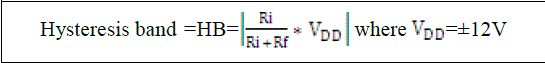
| The rectified sinusoidal hysteresis controller has an obligation of controlling and shaping the output current in such it matches the reference current. Fig.6. presents the conceptual diagram of the rectified sinusoidal hysteresis controller. According to Fig.6, the controller receives two inputs, the reference current (Iref) and the output current (Io). Iref is generated by the Arduino microcontroller. The output current (Io ) is measured and signal-conditioned by HCPL788J, an optical isolated sensor. A difference amplifier, OP-07D with unity gain, then subtracts both inputs; hence the error signal is generated by, Ierror = Io - Iref |
| The hysteresis controller, THS4021ID, compares the error signal whether it is out of the allowance gap or not, as referred in Fig.6. This allowable gap is referred from to Fig.7, is called “hysteresis gap” or hysteresis band (HB)”, and is defined by, |
 |
ZERO CROSSING DETECTOR
|
| The zero-crossing detector is a sensor which detects the rising edge of grid voltage; it generates the periodic pulse signal representing the frequency and the positive signal of grid voltage. This periodic signal is utilized in two control algorithms. First, under the current sink algorithm, the Arduino microcontroller detects it as the interrupt and starts executing the rest of the program after the interrupt have occurred. Second, it is used in islanding algorithm; this algorithm monitors the grid frequency and halts program if any fault conditions occur. According to Fig.8, the 220- Vrms grid voltage is attenuated to be a 9-Vrms voltage by a 50-Hz voltage transformer. The zener diode, 1N5231B, limits this attenuated voltage to a 5-Vpk signal. LM339, a quad-comparator IC, reconstructs this signal into a square wave signal. Finally, 74LS123, a monostable multivibrator, converts the square wave signal to the periodic pulse signal. |
MATLAB / SIMULATION RESULTS
|
| The inverter was implemented and simulated using the simulink and simpowersystem tool of MATLAB 7.10.0 (R2013a). Initially the solar radiation and temperature are given as an input to the PV model. According to the inputs given the PV panel produces an output voltage. The above fig.9 shows the simulation model single phase inverter connected with the RL grid. |
| The output of PV model is not constant and it is too small. So in order to boost up the voltage and make the output as constant irrespective of the change in temperature the boost converter is introduced. Then the boosted voltage is converted into AC component by using an inverter and the developed power is injected into the grid. From the fig.10 is gating pulses of the inverter switching module. |
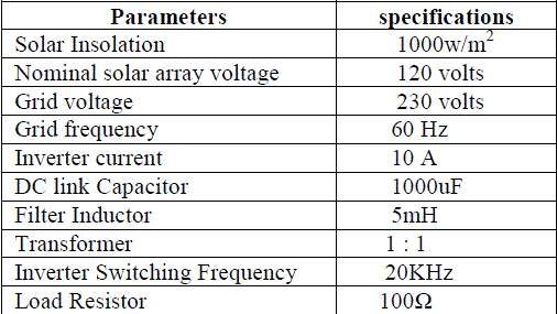
| The detailed parameters of the inverter, solar pv array, grid and other components specification are for simulation is shown in table. |
 |
| The Hysteresis controller is used to generate the PWM pulses. Fig.11 shows the MATLAB /simulink model of the hysteresis controller and Fig.12 and 13 are the input and output waveforms of the hysteresis controller model. |
| Grid current and voltage waveforms are shown in fig. 14. From this Fig Grid current and voltage waveforms are positive. So, the power at the input side of the inverter is positive. Hence we say that act as a source. When the grid voltage and inverter current both of them in-phase and it provides power factor is nearly unity. The current flows from the grid to inverter. Hence we absorb a power from the utility grid. So, our inverter acts as a load. |
| Grid current and voltage waveforms are shown in fig. 15. From this Fig we clearly examine that the voltage is positive and the current is negative ie., the current phase is shifted to 1800 (or) out of phase with grid voltage. So, the power is negative and therefore it acts as load. The current flows from the inverter to the grid. Hence we inject a power to the utility grid |
CONCLUSION
|
| The proposed design of single phase grid connected inverter system has been analysed and simulated by using MATLAB/SIMULINK. The output of solar PV power generation system is used to inject a power into the utility grid and it also used to feed a single phase residential load. Thus, this proposed configuration can greatly reduces the existing power demand, limits the use of conventional power generation techniques and also it is the only means to tackle the future power requirement. It saves the fossil fuels from depletion, limits global warming and keeps the environment clean and green. |
Figures at a glance
|
 |
 |
 |
 |
 |
| Figure 1 |
Figure 2 |
Figure 3 |
Figure 4 |
Figure 5 |
|
 |
 |
 |
 |
 |
| Figure 6 |
Figure 7 |
Figure 8 |
Figure 9 |
Figure 10 |
|
 |
 |
 |
 |
 |
| Figure 11 |
Figure 12 |
Figure 13 |
Figure 14 |
Figure 15 |
|
References
|
- Alamelu Nachiappan,Sundararajan.K and Malarselvam.V “Current controlled voltage source Inverter using Hysteresis controller and PI co ntroller”, IEEE, 2012.
- Omar David Munoz,”Design strategy for a 3- phase Variable Frequency Drive (VFD)”, senior project, Electrical Engg Dept, California polytechnic state University, San Luis obispo.2011.
- Li wang and Ying-Hao Lin, “Dynamic Stability analysis of a photovoltaic array connected to a Large utility Grid”, IEEE 2000.
- H.M.Abdar, A.chakravarthy, D.H.Moore, J.M. Murray and K.A.Loparo,”Design and Implementation a Specific Grid-Tie Inverter for an Agent-based Microgrid.
- Single-phase grid-connected photovoltaic system using rectified sinusoidal hysteresis current control, Mr. Chainon Chaisook, Assoc. Prof. Dr. Ake Chaisawad Dr. Veerapol Monyakul, Control System and Instrumentation Engineering, King Mongkut7s University of Technology Tho~lburi,2002
- Balaji Siva Prasad, Sachin Jain and Vivek agarwal, “Universal Single-Stage Grid connected Inverter”, IEEE Trans. Energy Convers, vol-23,no-1, pp.128-137,March- 2008.
- S.M.Cherati,N.A.Azli,S.M.Ayob and A.Mortezaei, “Design of a current mode PI controller for a Single-phase PWM Inverter”, IEEE Applied Power Electronics Collloquim(IAPEC)”, 2011.
- Power Electronics by M.H.Rashid.
- Power Electronics by Dr.P.S.Bimbhra, Kanna publishers, 4th Edition, 2010.
|