International Journal of Advanced Research in Electrical, Electronics and Instrumentation Engineering
ISSN ONLINE(2278-8875) PRINT (2320-3765)
ISSN ONLINE(2278-8875) PRINT (2320-3765)
Somnath Ganguly1, Joyti Mudi2, Soumen Paul3
|
| Related article at Pubmed, Scholar Google |
Visit for more related articles at International Journal of Advanced Research in Electrical, Electronics and Instrumentation Engineering
In this work the device measured voltage (phase to phase & phase to neutral) of sequentially, and give the output in the form of digitally. In this work three step down transformer is used for gets the different load voltage of three phase circuit, this voltage in going analog to digital converter circuit through the bilateral switch. The bilateral switch is operated through decade counter and the counter output is depending on the astable multivibrator. The output of astable multivibrator is controlled through RC constant.
Keywords |
| Analog to digital converter, bilateral switch ,decade counter, astable multivibrator. |
INTRODUCTION |
| Most of the electrical power generated in the world today is three-phase. Three phase power was first conceived by Nikola Tesla. In the early days of electric power generation,Tesla not only led the battle concerning whether the nation should be powered with low-voltage direct current or high-voltage alternating current, but he also proved that threephase power was the most efficient way that electricity could be produced, transmitted, and consumed. |
| In our work so far, we have considered both normal and abnormal (short circuit) operations of power system under completely balanced (symmetrical) conditions. Under such operation the system impedance in each phase is identical and the three phase voltage and current throughout the system are completely balanced, i.e. they have equal magnitude in each phase and are progressively displaced in time phase by 1200(phase a leads/lags phase b by 1200 and phase b leads or lag phase c by 1200). In a balanced system analysis can be proceed on the single phase basis. The knowledge of voltage and current in one phase is sufficient to completely determine voltages and currents in the other two phases. Real and reactive powers are simply three times the corresponding per phase values. |
| The system operation may also become unbalanced when loads are unbalanced as in the +’ 46+ presences of large single phase loads. Analysis under unbalanced conditioned has to be carried out on a three phase basis. Due to the unbalanced of the loads of the systems, the value of currents has been changed and also the voltage magnitude has changed. In this work the device measured the differential voltage (phase to phase or phase to neutral) of three phases sequentially, and gives the output in the form of digitally. |
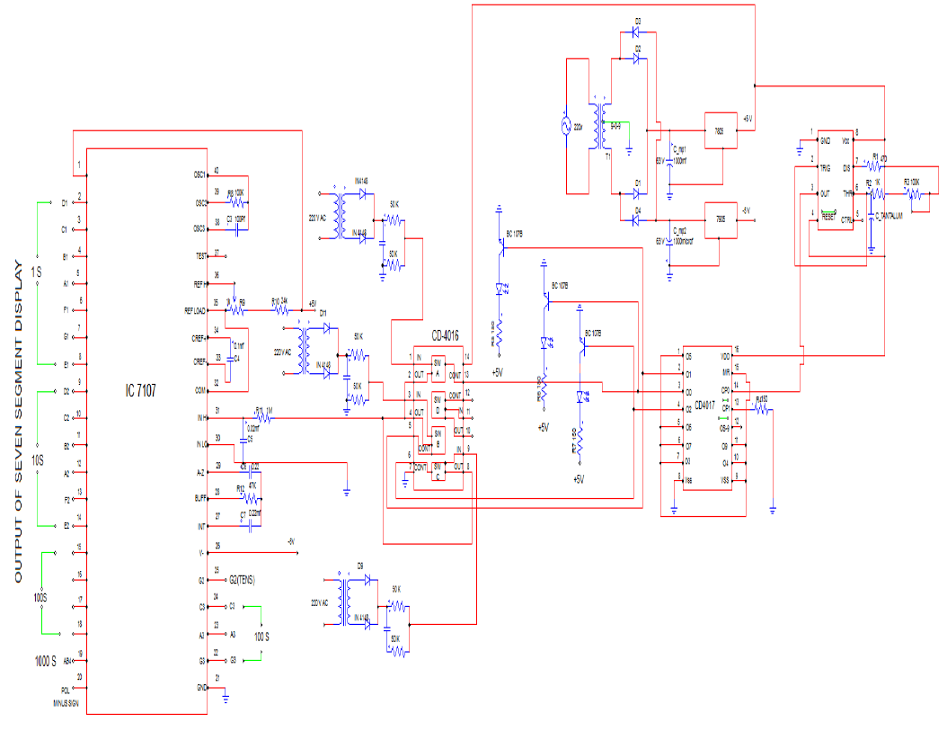
BLOCK DIAGRAM OF PROPOSAL MEASUREMENT SCHEME |
| In this voltage measurement scheme the seven block are represents the whole works (fig. 2). The first block is ± 5 V DC converter unit, this converter is converted 220 V AC to ± 5 V DC by the 7805 and 7905 ICs. The second block represent 555 timer in which the Astable Multivibrator is used by the suitable arrangement of the capacitor and register, that timer output is going on next block i.e. decade counter used as 4017 IC. The pulse of decade counter is going on the FET/bilateral switch i.e 4016 IC, that is connect with the three phase step down transformer. The output of 4016 IC is going on Analog to Digital converter in here 40 pin 7107 IC is used which convert analog to digital out puti.e display by the seven segment display. Each component of all blocks are derived in below: |
 |
WORKING CIRCUIT DIAGRAM |
 |
RESULT& ANALYSIS OF THREE PHASE VOLTAGE SCANNER |
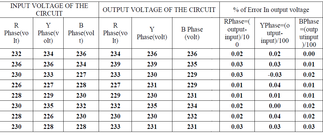 |
| When the input voltage of the circuit in R phase,Y phase and B phase are 232 volt,234 V and 236 V then the output voltage may be in R phase,Y phase and B phase are 234 V,236 V and 236 V.The percentage of error are calculated in three phase i.e in R phase,Y phase and B phase are 0.02%,0.02% and 0.00%.similarly when voltage varies in three phase i.e in R phase,Y phase and B phase(R phase 236 V,Y phase 236 V and 234 V) the output voltage of the circuit changes rapidly i.e in R phase,Y phase and B phase(R phase 239 V,Y phase 239 V and 235 V) and the percentage of error are taken as in R phase=0.03%,Y phase=0.03% and B phase=0.01%.similarly observed that changing the input values of R phase,Y phase and B phase,the output value changes and the percentage error increasing or decreaing with the reference of input. |
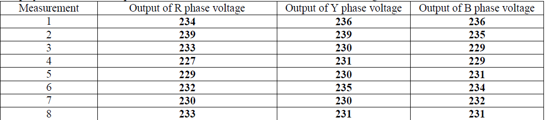
OUTPUT ANALYSIS OF THE THREE PHASE VOLTAGE SCANNER |
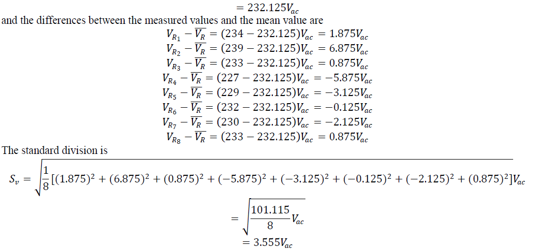
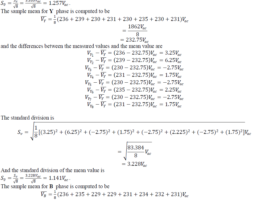
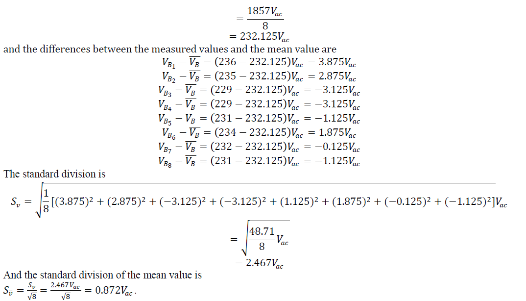
| In this works the outputs is analysis through statistical sample analysis. |
| In A.C voltage measurement are made to evaluate the repeatability of the AC voltage coming out of a seven segment display. The data will compute the mean value and standard deviation for the voltage data listed below. |
 |
| The sample mean for R phase is computed to be |
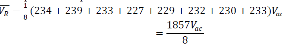 |
 |
| And the standard division of the mean value is |
 |
 |
CONCLUTION |
| In this works the device is measured analog a.c voltage value of the three phase system,to convert digital value. In this measurement one analog to digital converter i.c 7107 is used,thisic has 40 pin and output is tuned or calebrated through external RC circuit.Input of the i.c come through the step down transformer through the bilateral switch. The bilateral switch i.c 4016 is operated through decade counter i.c 4017 and the counter output is depending on the astable multivibrator. The output of astable multivibrator is controlled through RC constant. |
References |
|