International Journal of Advanced Research in Electrical, Electronics and Instrumentation Engineering
ISSN ONLINE(2278-8875) PRINT (2320-3765)
ISSN ONLINE(2278-8875) PRINT (2320-3765)
Abdul Kareem1, Mrs. E Kavitha2
|
| Related article at Pubmed, Scholar Google |
Visit for more related articles at International Journal of Advanced Research in Electrical, Electronics and Instrumentation Engineering
Reversible logic is one of the emerging technologies having promising applications in quantum computing. This project will deal with the design of a 16 bit reversible Arithmetic Logic Unit (ALU) with 15 operations is presented by making use of Double Peres gate, Fredkin gate, Toffolli gate, DKG gate and NOT gate. A new VLSI architecture for ALU using reversible logic gates is proposed. ALU is one of the most important components of CPU that can be part of a programmable reversible computing device such as a quantum computer. A first single bit reversible ALU and second single bit ALU are designed and Then 16 single bit ALU’s are cascaded together taking carry out of ALU performing LSB operation as an input to carry in of ALU performing next LSB operation. Design is implemented and verified in Verilog in modelsim Altera 6.6d.
Keywords |
| Reversible logic, Reversible ALU, MODEL SIM, Moore’s law. |
INTRODUCTION |
| It is well known that Moore’s law will stop to function sooner and something dramatic will therefore have to happen in microelectronics in near future. With much faster and more complex digital systems being built, power consumption of CMOS circuits has become a major concern. |
| Landauer [2] proved that power loss is an integral feature of irreversible circuits that have information loss irrespective of the technology the circuit is implemented in. |
| Also, Bennett [3] showed that in order to keep a circuit from dissipating any power, it had to be composed of reversible gates. |
| Reversible are circuits (gates) that have the same number of inputs and outputs and there is a one-to-one mapping between vectors of inputs and outputs. Thus the vector of input states can be always uniquely reconstructed from the vector of output states. Because truly low power circuits cannot be built without the concepts of reversible logic, various technologies and circuits for reversible logic are recently being studied [2]. |
| The Arithmetic Logic Unit (ALU) is essentially the heart of a CPU. This allows the computer to add, subtract, and to perform basic logical operations such as AND, OR etc. Since every computer needs to be able to do these simple functions, they are always included in a CPU. An ALU is a combinational logic circuit that can have one or more inputs and only one output. ALU’s output is dependent only on inputs applied at that instant as a function of time, and not on past conditions. A simple ALU in its basic form consists of two inputs for the operands, one input for selecting the desired operation and one output for the result. The complexity of ALU may vary from processor to processor. In [1], a reversible ALU for one binary arithmetic and three logical operations is designed in Base paper. In present work 16 bit ALU with 15 operations is design. |
RELATED WORK |
| Reversible Arthematic logic unit [1] with 4-operation AND, OR, X-OR and ADD. 4-bit adder/subtractor [7], Design of a 4-bit 2’s Complement Reversible Circuit [9], Design of Control Unit for Low Power ALU with a Barrel Shifter Using Reversible Logic [10], Design of 32 Bit Reversible ALU [11] with 7-operations and Arithmetic & Logic Unit (ALU), Design using Reversible Control Unit [12] with 9-operations are related and recent work in the field reversible logic circuits. |
REVERSIBLE GATES |
| Reversible logic gates Used in Design of circuit in this paper are NOT gate [8], Feynman Gate [4], Toffoli gate [5], Fredkin Gate [6], Double Peres gate [1] & DKG gate [7]. |
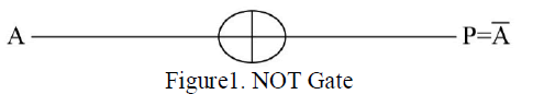
| NOT Gate [8] is a simplest Reversible gate and is a 1*1 gate. Not gate is shown in the Figure 1 and its quantum cost is Zero. |
 |
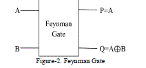
| FEYNMAN GATE [4] Controlled NOT (CNOT) gate is an example for a 2*2 gate. The Reversible 2*2 gate with Quantum Cost of one. It is shown in the Figure 2 |
 |
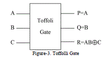
| TOFFOLI GATE [5] 2 CNOT gatesis 3*3 Reversible gate with three inputs and three outputs. Its quantum cost is 5 and is shown in Figure 3 |
 |
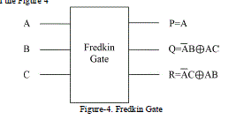
| FREDKIN GATE [6] is 3*3 gate maps inputs (A, B, C) to outputs (P=A, Q=A'B+AC, R=AB+A'C) having Quantum cost of 5 and It is shown in the Figure 4 |
 |
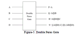
| DOUBLE PERES GATE [1] is 4*4 gate with quantum cost of 6. It is shown in the Figure-5 |
 |
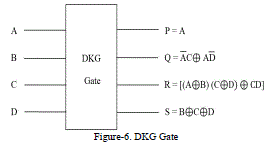
| DKG GATE [7] is 4* 4 reversible DKG gate [6] that can work singly as a reversible Full adder and a reversible Full subtractor is shown in Figure 6. It can be verified that input pattern corresponding to a particular output pattern can be uniquely determined. If input A=0, the proposed gate works as a reversible Full adder, and if input A=1, then it works as a reversible Full subtractor. |
 |
PROPOSED WORK |
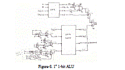
1-BIT-ALU |
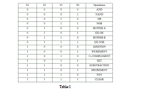
| The ALU that is proposed is 15-operations. ThereALU has 2 parts. 1st which has Double Peres Gate [1] as base of the circuit and is selected when select line s3 is zero. The operations performed here are buffer, AND, OR, NAND, NOR, EX-OR, and EX-NOR. 2nd part has DKG Gate as base of the circuit and is selected when select line s3 is one. The operations performed here are add, increment, 2’s complement, set, subtract, decrement, not, and clear. The operations selected depending on various select line are shown in the table-1 |
 |
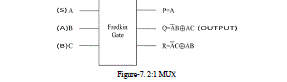 |
| The 2:1 Multiplexer is designed using Fredkin gate when we make A as select line and (B & C) as input. B or C is selected depending on A is 0 or 1 respectively. The block diagram is shown in figure 7. |
| Design of 1st1-bit ALU with 15 operations is shown in the figure 8. |
 |
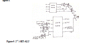
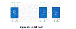
| For designing of 16-bit ALU we cascade 16 1-BIT-ALU as shown in the figure-10. We need to note here that only 1st bit has to be added with one for increment and 2’s complement or subtracted for decrement. There is slight change for SET and CLEAR operation also. Hence a different 1-BIT-ALU is designed as shown in figure 9 and cascaded from 2nd bit onwards till 16-bit. It is from (A1-A15) in the figure 10. A0 in the figure 10 is circuit shown figure 8. |
 |
 |
SIMULATION RESULT |
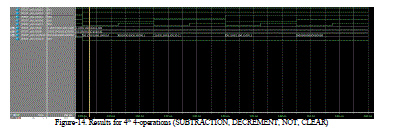
| The simulation result for code for 16-bit-ALU design written in Verilog and verified in model simaltera 6.6d is shown in figures (11, 12, 13 and 14). |
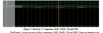 |
| Figure-11. Result for 1st 4-operations (AND, NAND, OR and NOR) |
| The Figure-11 shows the result of first 4 operations (AND, NAND, OR and NOR). These are operations are selected depending on select lines s3-s0 as shown in table-2. The Graph is shown each 4-operations because it can’t be accommodated in the same screen. In Present work the ALU is of 16-bit and has 15-operational features were as in the existing work the simulation result and design is for 8 to 10 features at the max. |
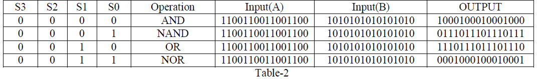 |
| Table-2 shows the first 4 operations selected depending on select lines. The operation is performed on2 input’s A & B and output is given out. |
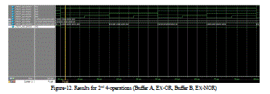 |
| The Figure-12 shows are result of second 4-operations (Buffer-A, EX-OR, Buffer B, EX-NOR).These are selected depending on select lines s3-s0as shown in the table-3 |
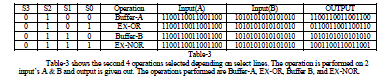 |
| Table-3 shows the second 4 operations selected depending on select lines. The operation is performed on 2 input’s A & B and output is given out. The operations performed are Buffer-A, EX-OR, Buffer B, and EX-NOR. |
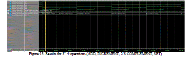 |
| Figure-13. Results for 3rd 4-operations (ADD, INCREMENT, 2’S COMPLEMENT, SET) |
| The Figure-13 shows are results of Third 4-operations (ADD, INCREMENT, 2’S COMPLEMENT, and SET).These are selected depending on select lines s3-s0 as shown in the table-4 |
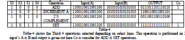 |
| Table-4 shows the Third 4 operations selected depending on select lines. The operation is performed on 2 input’s A & B and output is given out here Co is consider for ADD & SET operations. |
 |
| The Figure-14 shows the result of Fourth 4-operations (SUBTRACTION, DECREMENT, NOT, CLEAR). These are selected depending on select lines s3-s0 as shown in the table-4 |
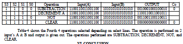 |
| Table-4 shows the Fourth 4 operations selected depending on select lines. The operation is performed on 2 input’s A & B and output is given out. The operations performed are SUBTRACTION, DECREMENT, NOT, and CLEAR. |
CONCLUSION |
| This 16-bit reversible Alu is designed and implemented in Verilog using MODEL SIM ALTERA 6.6d. The main aim of the design in this paper is improve the ALU features by increasing it to 15-operations and increase width to 16-bit. For further research this ALU can be extended to 32-bit and 64-bit and more features can also be added. |
| This design is verified using Verilog which has constrains of input to output one-way functionality, if we can design the reversible logic circuit using tools which support 2-way functionality the reversible logic result can be simulated and analysed in much better. |
References |
|