International Journal of Advanced Research in Electrical, Electronics and Instrumentation Engineering
ISSN ONLINE(2278-8875) PRINT (2320-3765)
ISSN ONLINE(2278-8875) PRINT (2320-3765)
Mr. Manjunath T.N1, Sunil T.D2, Dr. M. Z Kurian3, Imran Rasheed4
|
| Related article at Pubmed, Scholar Google |
Visit for more related articles at International Journal of Advanced Research in Electrical, Electronics and Instrumentation Engineering
The paper aims about the trace and debug of any N-bit controller using a JTAG, here controller core is traced using a interfacing device known as JTAG (Joint Test Action Group). JTAG is an advanced DFT Technique for the purpose of testing an ASIC, as such there are various technique for this purpose, but JTAG is chosen for its unique feature of in built state machine which can used for the purpose of both interfacing and display unit with a device as well as a testing device.
Keywords |
| JTAG ,DFT, Testing |
INTRODUCTION |
| The basic elements of boundary-scan architecture and its implications on the design of an integrated-circuit device. The rapid development of microelectronics technology, the integrated circuits become more complex with more functions and higher performances, but it also becomes more difficult to test the complex chips, so DFT (Design For Testability) circuits must be added to the chips during the design stage to reduce test costs. |
| This architecture defines the hardware and software for debugging and testing . It's a milestone event for DFT technology, and this architecture is approved as IEEE l149.1 protocol by IEEE organization. One of the most popular enhancement is on-chip debug by adding some JTAG instructions and special logics by analysing the design architecture and DFT schemes, one functional enhancement methodology to standard IEEE l149.1 JTAG controller will be proposed in this paper. Besides traditional boundary scan tests, this enhanced JTAG controller can also control internal scan tests especially provide the on-chip real-time debug feature to facilitate software development. |
| While going through this process the time taken to test and verify the design shall be reduced at least by 20% thus reducing the design cost when compared to the traditional methods of testing and debugging. |
MOTIVATION FOR BOUNDARY-SCAN ARCHITECTURE |
| The motivation for this paper is about the trace and debug of any N-bit controller using a JTAG here controller core is traced using a interfacing device known as JTAG (Joint Test Action Group). Since JTAG is an emerging and advanced DFT Technique for the purpose of testing an ASIC, almost in every controller applications JTAG ports are available with point of view JTAG based controller are designed. |
| In the current paper the enhancement on the JTAG feature is included with optimal speed and frequency. Designing of JTAG interface with the core and matching the baud frequency is Partially a challenging task. Hence try to increase the speed and performance compared to the previous version of JTAG interface. Solution Building the right interface with the JTAG controller and prototype on FPGA.This all flow and setup is built in the system on FPGA. |
| In the circuit testing with bed of nails has become increasingly untenable. The divide and conquer strategy of the bed of nails tester lets us the components in the circuits as if they were actually standing alone . surface mount technology with flat pack chip packages replaced dual in the packages because of a need to reduce inductance in the PCB by reducing the package height above the ground plane. |
| The in-circuit bed-of-nails technique relies on physical access to all devices on a board. For plated through-hole technology, the access is usually gained by adding test landing sites “lands” into the interconnects on the “B” side of the board that is, the solder side of the board. Board inductance is particularly an electrical problem at higher digital clock rates. |
| The advent of on asserted devices meant that manufacturers began to place components on both sides of the board the “A” side and the “B” side .The smaller pitch between the leads of surface mount components caused a corresponding decrease in the physical distance between the interconnects. It had serious impact on the ability to place a nail accurately onto a target test land. The whole question of access the compounded by the development of multi layer boards. |
PROPOSED WORK ON BOUNDARY-SCAN ARCHITECTURE |
| For the design and implementation of the Boundary Scan Register for Trace and Debug of Controller the proposed method is described below. The system will be designed and then described in Verilog description language. Then these descriptions will be processed by the standard Xilinx ISE 13.1 design tool suite. Synthesis, placement, routing and bit stream (FPGA physical programming information) generation will be done after that. Then the design would be ported on FPGA and the correctness of FPGA implementation has to be validated using simulation of Virtex-5 FPGA. |
| ClockIR-Clock for instruction register. Update,shift,capture are the state signals for FSM they can toggle to go either for high or low because they are the part of FSM. Enable TDO is test data out signal which should be 2-bit value this to enable the output of Tap controller. State and next state are the FSM state signals which are just 3-bit that represent the value of the states. Scan in is the scan signal meant for scanning the registers which should follow in TDO output. Data out should follow the same signals as that of IR Scan out and IR scan Register since it in scanning stage. |
| The collection of boundary scan Register is configured into a parallel-in, parallel-out shift register. A parallel load operation, called a capture operation, causes signal values on device input pins to be loaded into input cells and signal values passing from the core logic to device output pins to be loaded into output cells. A parallel operation called an update operation causes signal value present in the output scan Register to be passed out through the device output pins. |
| Data can also be shifted around the shift register in serial mode, starting from a dedicated device input pin called Test Data In and terminating at a dedicated device output pin called Test Data Out . The test clock, TCK, is fed in via yet another dedicated device input pin and the mode of operation is controlled by a dedicated Test Mode Select serial control signal. |
BOUNDARY- SCAN PATH |
| The boundary scan Register elements contribute nothing to the functionality of the core logic. The boundary scan path is independent of the function of the device. The value of the scan path is at the board level. This invention combines the best of the prior art by using the JTAG port to provide a means of communicating with a CPU in debug mode. Two additional test data registers are required in the JTAG logic together with CPU interface control logic. |
| The first added JTAG test data register is called the debug data register. It receives serial data from the JTAG test data input and transfers it to the CPU following the JTAG Update DR state. It is also loaded with data from the CPU at the JTAG Capture-DR states that data can be shifted out serially when the next data is shied in. This register is also part of the CPU register set but is available only when the CPU is in a special debug mode of operation. |
| The second JTAG test data register provides the additional status and control needed with this implementation. This register is called the debug status register .Breakpoint request-a control bit which requests an unconditional breakpoint.. Ready-a status bit which indicates that the CPU is trying to read an instruction or data from the debug data test data register. Freeze a status bit which indicates that the CPU is in debug mode. Debug mode enable a control bit which enables the CPU’s debug mode. |
| The CPU interface control logic and a communications protocol allow full duplex operation of the JTAG serial interface. the CPU interface decodes CPU accesses to the debug data register for instructions or data and sets the ready bit in the debug status register .When the JTAG TAP controller enters the Update DR state with the debug-data register selected the interface provides an acknowledge handshake back to the CPU to indicate that data is valid and the read cycle can be terminated. It also provides an acknowledge to the CPU when the CPU writes to the debug data register. |
| The protocol requires that the debug data register not be accessed by the JTAG test access port (TAP)controller until the CPU is trying to read an instruction or data from the debug data register. This is defined by both the freeze and ready bits being asserted in the debug status register. The protocol also requires that the CPU not perform more than one write to the debug data register between reads of the debug data register. |
| As in any embedded application written in ASM language it becomes tedious for the programmer to find the bug if the program is of greater size , so if the programmer is able to locate the exact location as where he/ she gone wrong it become easier to find bug . Keeping this in mind ,the core of the controller the program counter ,Register and the all the Ports of the controller are monitored, using JTAG and all the content of these ports are dumped onto a GUI , the GUI for this application was developed by the KEIL Software solutions. |
| It’s not only the process of finding error in the controller but also the testing the ASIC is possible, now this application is achieved by the BSR (Boundary Scan Reg) in built in JTAG .The only additional thing into added were two additional register Debug status and Debug data reg interfaced to the controller core .The Debug status register four control signal to control the controller operation and Debug data is meant to dump the core peripherals content and display onto GUI. |
| Thus for entire operation only a single in built state machine is used ,thus consuming less silicon and less no of pins, this methodology has incorporated two patents ideas. |
IMPLEMENTATION |
| The implementation of Boundary Scan Register is described in this section .The primary input signal and primary output signal is supplemented with a multi-purpose memory element called a boundary Scan Register. Cells on a device’s primary inputs are referred to as input register cells on primary outputs are referred to as output Register Input and output is relative to the core logic of the device. |
Synthesis Result : |
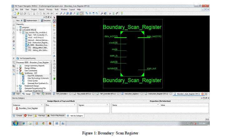 |
| ClockIR-Clock for instruction register. Update,shift,capture are the state signals for FSM they can toggle to go either for high or low because they are the part of FSM. Enable TDO is test data out signal which should be 2-bit value this to enable the output of Tap controller. State and next state are the FSM state signals which are just 3-bit that represent the value of the states. Scan in is the scan signal meant for scanning the registers which should follow in TDO output. Data out should follow the same signals as that of IR Scan out and IR scan Register since it in scanning stage. |
| Data can also be shifted around the shift register in serial mode, starting from a dedicated device input pin called Test Data In and terminating at a dedicated device output pin called Test Data Out. The test clock, TCK, is fed in via yet another dedicated device input pin and the mode of operation is controlled by the dedicated Test Mode Select serial control signal. |
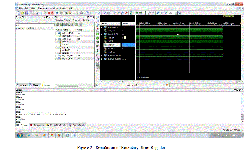
Simulation Result |
 |
ADVANTAGES |
| 1. Interfacing is easier using daisy chain architecture for parallel interfacing of multiple block. |
| 2. Testing and debugging is easier due to inbuilt JTAG TAP controller. |
APPLICATIONS |
| 1. Debugging ports in microprocessor. |
| 2. Debugging ports in microcontroller. |
| 3. Debugging ports in ARM. |
| 4. Debugging ports for any N-bit controller. |
FEATURES OF CONTROLLEER |
| 1. Fully Static CMOS Design Microcontroller |
| 2. Internal Oscillator with 24-42MHz of frequency range. |
| 3. 64K Bytes of In-System Programmable Flash for Application Program |
| 4. 256 Bytes of Internal RAM |
| 5. 8K Bytes of Auxiliary/External RAM |
| 6. Eight 8-Bit Bi-Directional Ports |
| 7. One Real-Time-Clock (RTC) |
| 8. Counts from a second to leap-year |
| 9. Alarm Setting Features |
| 10. Power Saving Features |
| 11. One Second clock taken as an interrupt source. |
| 12. Two 16-Bit Timer/Counters |
| 13. One Programmable Serial UART Channel |
| 14. One Master SPI Port |
| 15. One Master I2C Port |
| 16. Seven Interrupt Sources |
| 17. 256 Bytes deep of Hardware Stack |
| 18. Direct, indirect and relative addressing modes |
| 19. Power-On-Reset (POR) |
| 20. 50 ns Read Access Time for the Program Memory |
| 21. In-Circuit Serial Programming of the Flash Memory (ICFMPU) |
| 22. Code Protection |
| 23. Fully Compatible with the Industry standard MCS-51 |
| 24. Low-Power, High Speed CMOS FLASH Technology |
| 25. Low Power and Low Voltage Operations |
| 26. Package Type: 80 Pin TQFN |
CONCLUSION |
| An enhancement methodology to standard IEEE 1149.1 JTAG controller is proposed in this paper. With the enhanced features, all test functions including stuck at scan, memory BIST and high speed physical layer tests can be controlled by the JTAG controller besides traditional boundary scan tests, and further on-chip debug features are also integrated in this enhanced JTAG controller. Therefore, the chip costs can be reduced, and the software development and debug can be facilitated with the enhanced JTAG controller. The proposed approach will be implemented on FPGA and optimized for area, speed and power. |
| The Boundary scan has been implemented successfully in verilog. all other blocks will be developed and integrated to get the final output. |
References |
|