International Journal of Advanced Research in Electrical, Electronics and Instrumentation Engineering
ISSN ONLINE(2278-8875) PRINT (2320-3765)
ISSN ONLINE(2278-8875) PRINT (2320-3765)
| HinduBharathi P1, G Arun Sankar2 |
| Related article at Pubmed, Scholar Google |
Visit for more related articles at International Journal of Advanced Research in Electrical, Electronics and Instrumentation Engineering
This paper presents design and implementation of an Integrated Boost Resonant Converter (IBR) incorporated with Hybrid Frequency Modulation for photovoltaic applications. The designed Integrated Boost Resonant Converter employs a unique modulation method for extending the input range of Pulse-Width Modulation, low component count, galvanic isolation, simple control and high efficiency across a wide input and load range. The modulation technique includes primarily the hybridizing of constant-on, constant-off, and fixed-frequency control depending only on the required duty cycle. Effective Photovoltaic power conditioning requires efficient power conversion and accurate power point tracking to counteract the effects of panel mismatch, shading and general variance in power output during a daily cycle.
Keywords |
| Integrated boost resonant converter, Hybrid frequency modulation technique, Photovoltaic (PV). |
INTRODUCTION |
| Power conversion for photovoltaic (PV) applications, as opposed to more conventional dc–dc converter configurations, requires an adaptable system that is capable of responding to a wide range of input voltage and current conditions. PV voltage varies significantly with panel construction and operating temperature, while the PV current changes largely due to solar irradiance and shading conditions. If a converter is designed only for high peak efficiency, oftentimes the range of conditions common to many PV installations will force the converter into another operating region where it is much less efficient. Whether the input source is dynamic or the application calls for a universal input, the ability to maintain high-efficiency energy conversion over a wide range of conditions is a continual challenge. In many cases, extending the input range of a converter requires sacrificing conversion efficiency, or else adding a significant number of additional components. In photovoltaic (PV) applications, efficient, low-cost enhancements to improve converter efficiency are desirable. |
| One such method of enhancing converter operation is the selection of an appropriate modulation scheme. In this paper, a unique dc–dc converter modulation scheme is proposed for a class of converters that integrate PWM stages into unregulated resonant converters. The resonant stage provides galvanic isolation with high efficiency, while the PWM stage provides the necessary regulation. Though the efficiency is good with a narrow input range and fixed-frequency PWM, it is still possible to extend the operating range while maintaining high efficiency. This new method, a hybrid between constant-on, constant-off and fixed-frequency modulation, optimizes the converter efficiency at the nominal line input while allowing an extended input range. In the distributed PV PCS, the isolated dc–dc stage must operate efficiently at full power, while maintaining high performance at light load, across a range of PV voltages. In order to maintain high efficiency under low-power conditions, it is necessary to minimize the amount of circulating energy in the system. |
| One popular option for the dc–dc conversion stage is a simple continuous-conduction-mode flyback converter, It has the benefit of simple construction and low circulating energy. However, the switching loss for both the primary switch and the diode can be quite large, and the overall system efficiency is typically low (<90%) [2]. Improvements in flyback efficiency can be made using variants such as zero voltage transition or active clamp, both of which use the transformer leakage inductance as a resonant element to achieve zero-voltage switching (ZVS) across the main device. However, this effectively trades switching loss for circulating energy, reducing efficiency at high line or low power [5]. |
| Another option is the series-resonant converter, and more recently the LLC resonant converter, both of which operates on a similar principle and, typically, use a variable frequency control to adjust the output voltage. When the seriesresonant, or LLC converter, is operated near the resonant frequency of the tank circuit, the converter achieves nearly ZVS and zero-current switching (ZCS) with very low circulating energy, giving it a high peak efficiency. However, as the operating frequency diverges from the resonant frequency, the amount of circulating energy increases. Unfortunately, the normal conditions for PV conversion will often push the converter significantly away from the optimum switching frequency, causing the CEC efficiency to suffer [4]. Several authors have proposed methods to extend the line and load range of the LLC, once again complicating the circuit topology and control [3]. The method proposed in this paper integrates a traditional boost converter element into the DCX with only the addition of a single inductor. The overall design is straightforward and may be controlled Hybrid frequency PWM with only the need to observe limitations on the maximum and minimum duty cycle[1]. For PV applications, this circuit satisfies the need for galvanic isolation, low switching loss, minimal circulating energy, as well as simple gate drive and control. |
 |
CONVERTER SYNTHESIS AND OPERATION |
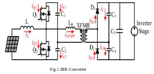
| The proposed modulation scheme is developed primarily for circuits that employ this integration of PWM and resonant conversion. One such circuit is the integrated boost resonant (IBR) converter, which is shown in Fig.1. The IBR’s rectifier capacitors, C1–C4, are sized appropriately so that they resonate fully with the transformer leakage inductance during each half of the switching cycle. This resonant action occurs simultaneously with a synchronous boost circuit formed by the input inductor and the two MOSFETs Q1 and Q2. The two MOSFETs are switched complementary to one another in the proceeding analysis, with the duty cycle D defined for the lower switch Q2. Thus, the boost action is said to be integrated into the resonant converter. Allowing this resonant action to complete fully adds four primary benefits, |
| 1) the output diodes D1 and D2 achieve zero current switching (ZCS); |
| 2) switching loss in the primary-side MOSFETs is equal to a normal synchronous boost; |
| 3) the transformer has zero circulating energy; |
| 4) the resonant stage gain is fixed and equal to the transformer turns ratio (1:n). |
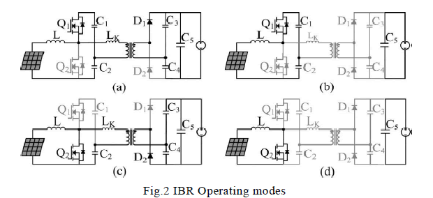 |
A. Mode 1 [t0 < t < t1; in Fig. 2(a)]: |
| Beginning with the turnoff of Q2 prior to t0 , the current in the input inductor L flows into the body diode of Q1 , discharging its parasitic capacitance. This allows Q1 to be turned ON under ZVS conditions at t0. At this time, the upper input-side capacitor C1 begins resonating with the transformer leakage inductance Lk and the output-side capacitors, C3 and C4, through D1 . Simultaneously, the input current begins charging the series combination of C1 and C2. During this phase, Q1 carries the difference between the transformer current, flowing from C1 through the positive terminal of the transformer and the input current. Once the transformer current resonates back to zero, D1 prevents the continued resonating in the reverse direction, ending mode 1. |
B. Mode 2 [t1 < t < t2; Fig. 2(b)]: |
| Q1 is still active, yet it is only conducting the input inductor current, which is still decreasing, a pathway which is shown in Fig. 4(b). The resonant elements all conduct zero current during this interval. Only C5 continues discharging into the load at this time. Mode 2 ends with the turn-off of Q1 and the subsequent turnon of Q2. |
C. Mode 3 [t2 < t < t3; Fig. 2(c)]: |
| After the turn-off of Q1 , but prior the turn-on of Q2 , the inductor current is still shunted into charging the series combination of C1 and C2, this time through the body diode of Q1 , and still decreasing almost linearly. When Q2 is turned ON, the body diode of Q1 is hard commutated, causing some switching loss. At t2, C2 begins to resonate with Lk and the parallel combination of C3 and C4 , through the diode D2 . Simultaneously, the inductor current also flows through Q2, increasing linearly. During this interval, Q2 carries the sum of the transformer current and the inductor current. Thus, the rms current through Q2 is significantly larger than that of Q1, which carries the difference of the two currents. Once the transformer current resonates back to zero, D2 blocks the continued oscillation, marking the end of mode 3. |
D. Mode 4 [t3 < t < t4; Fig. 2(d)]: |
| The inductor current continues to flow through the lower device, increasing until Q2 is turned OFF and the circuit returns to mode 1. Also, during both modes 3 and 4, Q1 effectively isolates the upper capacitor from charging or discharging. |
DESIGN PROCEDURE |
A. DeterminingDutyCycleLimitsFromInputRequirements: |
| The most critical element of this design procedure is the identification of the input voltage requirements, so that the duty cycle range is fully utilized. With this converter, there is a direct tradeoff between increased input range and lower rms currents in the circuit. The most basic method involves setting the maximum and minimum duty ratios such that the middle of the input range results in a 50% duty cycle at the converter. |
 |
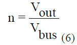
| With the nominal input assigned to have a 50% duty cycle, the bus voltage Vbus which is measured across C1 and C2 can be calculated by |
 |
B. Determining Maximum Resonant Period Lengths |
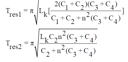
| With the maximum and minimum duty ratios known, thelimits for the resonant periods Tres1 and Tres2 may be calculated based on the desired sw00itching period Tsw utilizing the following equations: |
 |
C. Design Transformer |
| Based on the calculated Vbus and the desired output voltageVout , the following equation can be used to calculate thenecessary transformer turns ratio, n: |
 |
| The transformer design process can be carried out under anumber of different procedures; however, the peak V–S product, provided in the following equation, is often a useful quantity when determining the transformer flux density, core size and number of primary turns: |
 |
D. Design Input Inductor Based on Allowable Current Ripple |
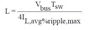
| Multiple criteria may be used for designing the input inductor.In PV applications, especially for accurate MPPT, the inductor current ripple must be regulated. The following equation specifies the input inductance based on the maximum allowable current ripple (which occurs at D = 0.5) |
 |
E. Resonant Capacitor Design |
| With the magnetics design complete, it is now possible todesign the resonant capacitorsC1–C4 . In order to reduce the rmscurrents in the circuit, the resonant period needs to be as close to the calculated maximum as possible. Because the leakage inductance of the transformer, Lk , is involved in the resonant circuit and is a consequence of the transformer design in step C, it is left as a constant here. The full equation for calculating Tres1 is given in (4). If the duty cycle was not adjusted as in the second half of step 1, then Tres2 is not necessary to design. |
 |
F. Average Diode Current |
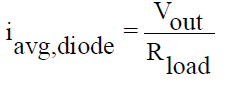
| The output diodes D1 and D2 need to block the full output voltage. The average current they need to carry is given as |
 |
| In order to overcome the drawbacks of traditional PWM, other modulation methods have been proposed, three of the most popular being constant-on, constant-off, and hysteretic control. For the IBR, constant-on modulation provides a selectable minimum on-time that can ensure ZCS during at least one-half cycle. There is no controllable off-time, however; therefore, ZCS is only guaranteed for the output diode for duty cycles greater than 50%. Also, constant-on control requires an extremely wide frequency range, with the maximum frequency occurring only at the minimum input voltage. Similarly, constant-off control provides only a selectable off-time, guaranteed ZCS for only duty cycles less than 50%, with the maximum frequency occurring at the maximum input voltage. With hysteretic control, there is no minimum on- or off-time and no guarantee of ZCS. In order to improve the utilization and efficiency of the IBRconverter under a wide load range, the designed modulation scheme needs to have a selectable minimum on- and off-time, guaranteed ZCS across the operating range, narrow operating frequency band, and maximum frequency occurring at 50% duty cycle so as to minimize the transformer core loss. The input voltage reference is generated by the maximum-power-point tracking (MPPT) loop, passing a reference to the input voltage control loop. The normal output of the digital compensator is the only required input to the hybrid frequency modulator, and the output works naturally with a PWM comparator that requires both a switching period length and a value for the main switch on-time. |
SIMULATION OF STUDIES |
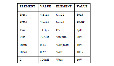
| Table1. POWER STAGE ELEMENT VALUES FOR 250-W PROTOTYPE |
 |
| In order to evaluate the effectiveness of the proposed method the drive system shown in fig. 3 was simulated by POWERSIM. |
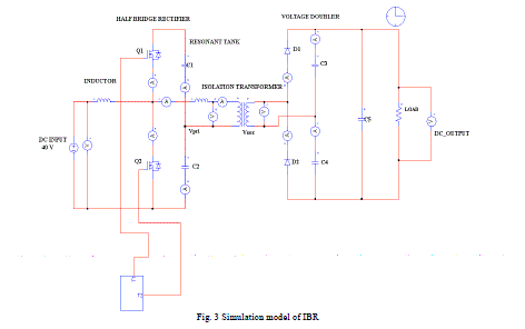 |
| Fig. 3 Simulation model of IBR |
 |
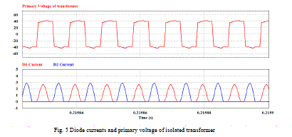 |
| Fig. 5 Diode currents and primary voltage of isolated transformer |
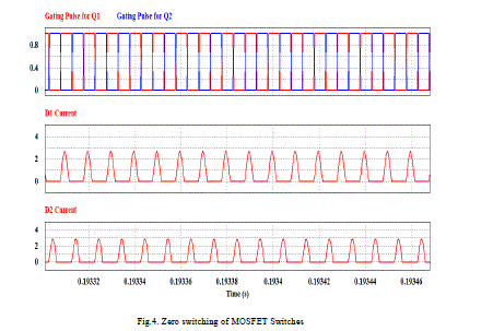
| There is a significant difference in the circuit behaviourbetween the two resonant modes (1 and 3). During mode 3, C1 is effectively isolated from the rest of the circuit due to the presence of Q1. However, during mode 1, C2 has an acdischarge path through the PV source and the input inductor, allowing the two input capacitors (C1 and C2 ) to appear in parallel, though the resonant current is not shared evenly between them. Thus, the length of mode 1 can be significantly longer than mode 3 as in Fig. 4 and Fig. 5, depending on the relative sizing of C1–C4 and the transformer turns ratio n |
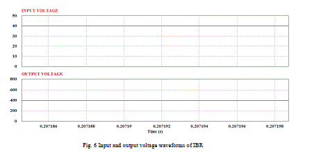 |
| Fig. 6 Input and output voltage waveforms of IBR |
| A Solar module which has open circuit voltage of 42V is interfaced with an IBR which is shown in the Fig 6. An IBR boosts up the input from PV module and Inverter converts this DC voltage to AC voltage. MPPT tracking is used to obtain maximum power from PV module. |
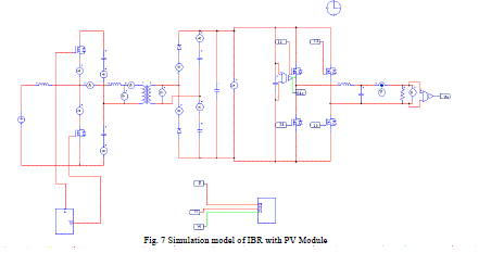 |
| Fig. 7 Simulation model of IBR with PV Module |
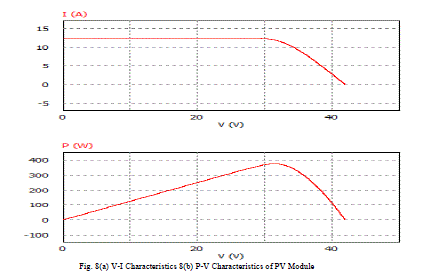
| The V-I and P-V characteristics of PV Module are shown in Fig 8(a) and 8(b) respectively. |
 |
| The Output AC Voltage waveform of overall IBR system with PV module is shown in the Fig 9. |
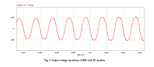 |
| Fig. 9 Output voltage waveform of IBR with PV module |
CONCLUSION |
| As a solution for providing efficient, distributed PV conversion,an isolated boost resonant converter has been proposed. The system is a hybrid between a traditional CCM boost converter and a series-resonant halfbridge, employing only two active switches. The synthesis of the converter was described along with the circuit operating modes and key waveforms In order to extend the line range of the IBR converter while maintaining high weighted efficiency, a special hybrid frequency modulation scheme is proposed. The scheme reduces core and conduction loss dramatically by decreasing the applied volt-seconds at the transformer and improving the switching period utilization. With hybrid frequency control, the circuit also maintains ZCS for the output diodes, minimizes switching loss, and eliminates circulating energy at the transformer across the entire operating range. It also allows for a predictable voltage gain, dependent only on duty cycle and transformer turns ratio. The principle advantages of utilizing this topology wereas follows: |
| 1) high weighted efficiency because of low circulating energy and reduced switching loss with resonant energy transfer and output diode ZCS; |
| 2) lowpotential cost due to minimal number of active devices and a small overall component count; |
| 3) galvanic isolation allows for the use of high efficiency inverter stages without additional concern over ground leakage current; |
| 4) reduced control complexity provides lower auxiliary power loss and simpler controller IC configurations. Finally, simulation verification of proposed modulation method was presented. |
References |
|