International Journal of Advanced Research in Electrical, Electronics and Instrumentation Engineering
ISSN ONLINE(2278-8875) PRINT (2320-3765)
ISSN ONLINE(2278-8875) PRINT (2320-3765)
Harish D1, Somsing Rathod2, Amit Goel3, Dr.G.Sadashivappa4
|
| Related article at Pubmed, Scholar Google |
Visit for more related articles at International Journal of Advanced Research in Electrical, Electronics and Instrumentation Engineering
Transmit/Receive Modules (T/R Modules) are vital parts of modern phased array radar systems. The T/R modules are controlled using T/R module controllers (TRMC’s) which generate the necessary control signals for beam steering and calibration. Present day TRMC’s are FPGA based Dual T/R module controllers (DTRMC’s). A single DTRMC controls two T/R modules. In this paper we propose the design and implementation of ASIC (Application Specific Integrated circuit) to replace the existing FPGA based DTRMC’s. Also the controller is designed as a Quad TRMC (QTRMC) capable of controlling four T/R modules. The design of the major blocks (UART and Decoding logic) of the controller are discussed. The design is carried out in VHDL and simulated using Xilinx 12.4 with Spartan 3E XC3S250E-5ft256 as target device.
Keywords |
| T/R module,QTRMC, UART |
INTRODUCTION |
| A phased array is a directive antenna composed of a number of individual radiating elements each of which is fed with a phase shift. The radiation pattern of such radars is determined by the amplitude and phase of the current at each of its radiating elements. The phased array antenna has the advantage of being able to have its beam electronically steered in angle by changing the phase and amplitude of the current at each element. The phase shift that is given to and power to be radiated by each element is controlled by the Beam Steering Unit (BSU). The beam of a large phased-array antenna therefore can be rapidly steered from one direction to another without the need for mechanically positioning a large and heavy antenna. Amit Bisht, Somsing Rathod, Varadarajan and Yogeesh Kumar [1] proposed the FPGA T/R Unit Controller (TRUC), which controls 2-T/R modules packaged in a single housing. Two such controllers are integrated in each of the TRU and interfaced over a l0-Mbps duplex serial link (multi drop LVDS bus interface). This controller generates the necessary control signals required for normal and calibration operation as well as monitors the status of the T/R modules. |
| Advanced long range Active Phased Array radar systems are composed of large number of solid state T/R modules in order to achieve high power aperture product. Nicholas J. Kolias and Michael T. Borkowski [3] discuss regarding the development of T/R modules for Active Electronically Steered Arrays (AESA’s) The key enabler for the AESAs has been the development and improvement of the performance, manufacturing capability, and cost of the Transmit/Receive (T/R) modules that typically sit behind each radiating element of the array The prime requirement of these radars is low side lobe level and fast target update rates. The above mentioned requirements are met by controlling the phase and amplitude of the T/R modules distributed in the Active phased array radars. In order to form a beam the T/R modules should be assigned with specific phase shift value. Sundaraman [4] propose the 6 bit phase calculation in the T/R module controller from the 16 bit word received from the high level controller. T/R modules provide a much higher bandwidth and higher average transmit power when compared to passive phased array radars. Also T/R modules provide increased radar sensitivity in the range of 8-12 dB as compared with passive arrays. |
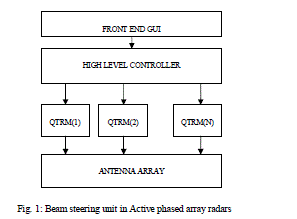 |
| Fig. 1: Beam steering unit in Active phased array radars |
| The beam steering unit in fig 1 shows the distributed architecture in an Active phased array radar and the location of various components of the radar |
TRANSMIT/RECEIVE MODULE |
| In an active phased array radar a single T/R module is used with each radiating element. T/R modules set up the system performance in a phased array radar. The first T/R modules were developed by Texas Instruments as part of the United States Air Force’s molecular electronics for radar applications program. The main components of a T/R module controller include phase shifter, power amplifier, low noise amplifier, duplexer, attenuator and protection circuit to avoid any leakage of the transmitted pulses into the receiver through the duplexer. |
| The major three functions of a T/R module are |
| a) To boost output power of transmitted signal up to its final radiated power. |
| b) Establish system noise figure for reception. |
| c) Provide beam steering. |
T/R MODULE CONTROLLER |
| The schematic diagram of the T/R module controller (TRMC) is as shown in fig 2. The T/R module controller interfaces with the higher level controller over the LVDS ( Low Voltage Differential Signaling) interface. LVDS has advantages such as low power requirements and reduced interference. Communication takes place in LVDS over a differential pair of wires. The TRMC internally can be divided into three major sub blocks namely the UART, Decoding logic and the Control logic. The various inputs and outputs of the TRMC is as depicted in fig 2. The SIN is the serial data input line which is connected to the 16 bit UART of the TRMC. The RST (reset), TRP (T/R pulse) and SOB (Start of Beam) are control signals which synchronize various operations inside the TRMC. The TEMP input gives the temperature status of T/R modules. PWR OUT is the transmitted RF power which is monitored by the TRMC. Also various DC supplies are monitored by the controller through the DC STS (DC supply status) input. In the output side the TRMC which is Quad controls four T/R modules and thus has four 6 bit phase shifter lines (PH1 to PH4) and four 6 bit attenuator lines (ATT1 to ATT4). |
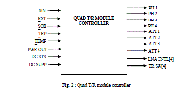 |
| Fig. 2 : Quad T/R module controller |
UNIVERSAL ASYNCHRONOUS RECEIVER TRANSMITTER (UART) |
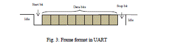
| UART is a type of serial communication protocol, often used for short distance, low cost, low speed data exchange between computer and peripherals. The major components of a UART are the baud rate generator, receiver and transmitter. UART allows full duplex communication and is thus used for data exchange between a set of devices.The frame format of data exchange using UART is as shown in fig 3 . The first bit in the frame is a low bit which indicates the start bit of the frame. The bits succeeding the start bit is the data of interest. The last bit of the frame is the stop bit which is a high bit |
 |
| The onboard clock is 50 Mhz, UART cannot operate at such high data rates thus there is a need for converting the onboard clock frequency to lower rates usable by the UART. In the present design the need of baud rate is 5Mbps thus the clock frequency of 50 Mhz has to be converted to 5 Mhz. This can be achieved by dividing the clock frequency by a factor 10 using a decade counter. |
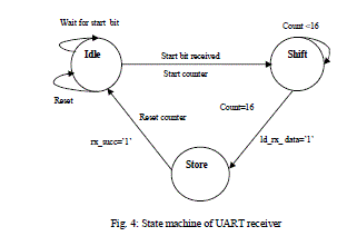
| During reception in the UART, serial in parallel out (SIPO) procedure is followed. It consists of three states namely idle, shift and store as shown in fig 4. In the idle state the counter is reset and the UART is waiting for a high to low signal i.e the start bit. The idle state is entered upon reset also. Once the start bit is received the counter begins counting the samples and the state transits from idle to shift state. In the shift state the serial data which is input is stored using a temporary shift register. The bits are shifted until the counter reaches 16 and the stop bit is received. Upon reception of the stop bit the state transits from shift to store where the contents of the temporary register is copied to the main register rx_data and the counter is stopped. |
 |
| During transmission from the UART, parallel in serial out (PISO) is process is done. It consists of three states namely Idle, load and shift as shown in fig 5. In the idle state the transmitter waits for a low to high transition of the tx_enable signal. The idle state is also enabled upon reset. When the tx_enable goes high, the state shifts from idle to load data and the data to be transmitted is loaded to a temporary register and then a start bit is inserted (i.e a high to low signal) into the serial out line ‘sout’ and the counter is started. Now the state transits from load data to shift. |
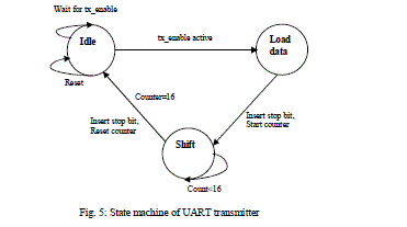 |
| The state machine remains in this state until the counter reaches the value 16. When the counter reaches 16 a stop bit i.e a high signal is inserted to the ‘sout’ line and the counter is reset. The counters used for the transmitter and receiver are 5 bit counters |
DECODING LOGIC |
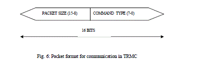
| In any active phased array radar it is very much necessary that all the calibration and beam steering command are applicable to the Transmit/Receive module. Transmit/Receive module has to function as per the radar requirement in terms of switching from Rx/Tx and vice versa. Active module protection and status is also required for reliable and proper function of radar system. All these functionality Rx/Tx switching, T/R module protection and T/R module status is implemented in controller card. Which acts based on commands received from interconnected subsystems in the radar. The commands are decoded based on the packet size contained in the header of the packets (fig 6) . The UART performs the task of receiving serial data at 5 Mbps from the higher level controller and converting the serial data to parallel for decoding and control purposes. |
 |
SIMULATION AND RESULTS |
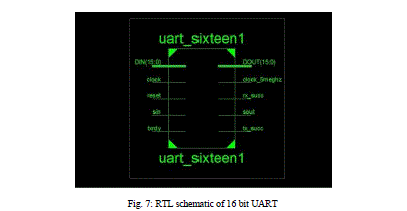 |
| The RTL schematic of the simulated 16 bit UART is as shown in fig 7. Here ‘sin’ is the serial input line and ‘sout’ is the serial output line. DIN and DOUT are 16 bit registers used during transmission and reception respectively |
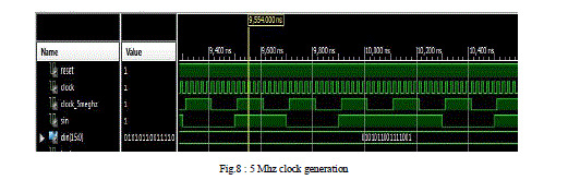
| The clock divider design simulation for the conversion of 50 Mhz onboard clock to 5 Mhz is as shown below in fig 8. By using a decade counter the 5 Mhz port line is inverted for every 5 cycles of the master clock |
 |
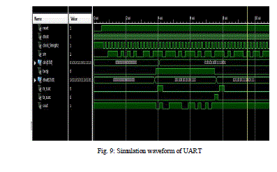
| The simulation waveform of the UART is as shown below in fig 9. tx_succ and rx_succ are signals which indicates the successful transmission and reception of data words.The txrdy is the transmission enable signal which helps prevent transmission of junk data over the sout line. The sout line is held high by default when there is no transmission. |
 |
| For the decoding of packet size from the command word sent by the higher level controller a VHDL code is written and this is instantiated in the main file of the decoding logic by structural coding methods of VHDL. A decoding enable signal is set high whenever the machine transits from the idle state. Upon this transition, the contents of the register which receives data from the UART is loaded to a temporary register for decoding the packet size termed as deco_reg as shown in figure 10 and 11. The RTL schematic is shown in fig 10. |
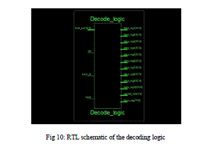 |
| Fig 10: RTL schematic of the decoding logic |
| The decoding process is started after the data is written to the decoding register. The bits 15 downto 8 is taken and processed by means of a function which converts the value in binary to an integer. The result obtained is stored in a variable termed as packet_size as shown in figures 10 and 11 and further the state machine transits based on this signal value. |
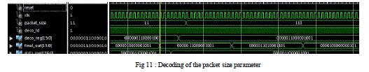 |
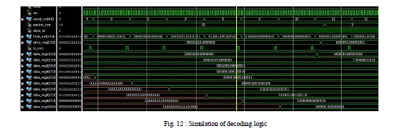
| The range of the packet size value is limited from a minimum of 3(0011) to a maximum of 10 (1010) for various commands intended for the T/R modules. Based on the packet size the ten data registers are updated with new data. Not all the data registers are updated all the time but the number of registers equal to the packet size are updated as shown in figure 12. |
 |
| It can be seen from the simulation waveforms of figure 11 that the packet written to the decoding register is 0A80. Thus the decoder decodes the packet size as 0A which is equal to 10. Hence all the 10 data registers are updated with the subsequent data. Thus as compared to the existing DTRMC which controlled only two T/R modules, in this design the transmit/receive phase and attenuation values for each of the four T/R modules can be stored in the registers after decoding for loading onto the phase and attenuation registers upon the command fromthe higher level controller. |
CONCLUSION |
| The heart of the Quad Transmit receive module controller, the UART was designed and tested for 5 Mbps operation using the clock divider. The decoding logic block successfully decodes the packet size parameter contained in the packet transmitted from the high level controller over the UART and updates the appropriate number of registers. The updated register values can be input to the control logic of the QTRMC and in turn the phase and attenuation registers will be loaded with the desired values for beam steering. |
References |
|