International Journal of Advanced Research in Electrical, Electronics and Instrumentation Engineering
ISSN ONLINE(2278-8875) PRINT (2320-3765)
ISSN ONLINE(2278-8875) PRINT (2320-3765)
P.Premkumar1, Dr.S.Kavitha2, S.Nandhini3
|
| Related article at Pubmed, Scholar Google |
Visit for more related articles at International Journal of Advanced Research in Electrical, Electronics and Instrumentation Engineering
Modern DSP systems are often well suited to VLSI implementation. Indeed, they are often technically feasible or economically viable only if implemented using VLSI technologies.. The paper is focused on the design of an efficient VLSI architecture for FIR filters which aims at reducing the power consumption and also to reduce the hardware complexity. In the existing method, design of folded FIR filter based on conventional multiplier is presented. It does not allow the internal pipelining delays to be exploited. It leads to significant increase in hardware as well as considerable increase in power consumption. It leads to less throughput and increases hardware complexity. In the proposed method, design of folded finite-impulse response (FIR) filters based on pipelined carry-save multiplier is presented . The design is considered at the bit-level and the internal delays of the pipelined multiplier array are fully exploited in order to reduce hardware complexity. Partially folded architectures are also proposed which are implemented by cascading a number of folded FIR filters. The proposed schemes are compared as to the aspect of hardware complexity with a straightforward implementation of a folded FIR filter based on the conventional multipier . The comparison reveals that the proposed schemes may require 20%–30% less hardware. Due to the lesser carry propagation, the proposed method can achieve low power consumption and higher computational speed strategy.
Keywords |
| Folding, FIR Filters, Multipliers, Tanner EDA. |
I.INTRODUCTION |
| Nowadays, digital signal processing (DSP) is used in a wide variety of real-time applications and is playing an important role in the digital revolution. Finite-impulse response (FIR) digital filters are the most fundamental DSP components. FIR filters have the advantage of stability and easy implementation but the large number of filter taps leads to excessive hardware complexity. Power consumption is another important factor in DSP circuits, especially when used in mobile communication systems. |
| Folding techniques have been proposed as a means of reducing hardware when the processing throughput required by the application is less than the throughput at which the circuit can operate. FIR filters are ideal candidates for folding since they are essentially a repetition of multiplications. A reconfigurable folded transposed FIR filter architecture has been presented in but not detailed implementation is given, although the bit-level design can lead to hardware efficient circuits. An important issue in synchronous designs is the avoidance of problems related to clock-skew. A number of asynchronous architectures have been presented in the bibliography as a solution to this problem at the expense of extra hardware. A significant advantage of the folded FIR architectures is that they lead to reduced hardware in comparison with the corresponding unfolded schemes and the clock-skew problem does not exist. Thus there is no need to resort to hardware expensive asynchronous solutions.[1] |
| Due to the lesser carry propagation, the proposed method can achieve low power consumption and higher computational speed. The circuit is simulated in T-Spice in 180 nm technology. Power estimation can be obtained through transistor level design simulation. |
II.RELATED WORKS |
| Osman Hassan and Skander kort presented a formal synthesis methodology that is capable of performing correct synthesis at almost all levels of abstraction and can be adapted to be used for most of the combinational digital circuits irrespective of their size and complexity. The proposed methodology calls for proving the correctness-preserving characteristic for the transformations that are required in the synthesis of a particular digital circuit in a higher-orderlogic theorem prover. |
| Parate and Patil presented the paper on several experimental systems based on programmable logic have been designed and implemented which are programmed using a hardware design methodology. One necessary component of the software environment will be a library of standard macrocells corresponding to commonly used arithmetic and logical operations. In this paper Array multiplier is designed specially for programmable logic. |
| Li-Hsun Chen, Oscal -C. Chen developed a low-complexity and high-speed transposed direct-form finite-impulseresponse (FIR) architecture is based on the radix-4 Booth algorithm. It includes a pre-processing unit, Input sub-data latches, a control unit, and booth decoders, filter coefficient registers, an accumulation path and a post-processing unit. |
| Amir Khatibzadehl, Kaamran Raahemifar, Majid Ahamdi describes a design of 8-bit x 8-bit unsigned multiplier. Highthroughput rate is achieved by a new architecture implementing our earlier multiplication technique [1] in conventional register pipelining at the bit level. The multiplier is designed in 0.18-pm CMOS process. HSPICE simulation results indicate that our multiplier operating rates up to 6 GHz under the supply voltage of 1.8V. |
| Rizwan Mudassir and Z. Abid explained a two new parallel multiplier architectures are designed based on two new full adders. These two adders are based on a new algorithm and display low power dissipation and high speed. The compactness and regularity of conventional array multipliers are maintained. The partial products are generated more efficiently using lower number of transistors. The proposed two multipliers offer significant improved performance, in terms of speed and power dissipation, than standard array multipliers[9]. |
| A.P. Vinod, A. Singla and C.H. Chang, presented a minimal-difference differential coefficients method for low power and high-speed realisation of differential-coefficients-based finite impulse response filters. The conventional differential coefficients method (DCM) uses the difference between adjacent coefficients whereas we identify the coefficients that have the least difference between their magnitude values and use these minimal difference values to encode the differential coefficients. |
III.PROBLEM STATEMENT |
| The elaborate design of folded FIR Filter is considered. In the existing method, it does not allow the internal pipelining delays to be exploited. It leads to significant increase in hardware as well as considerable increase in power consumption. It leads to less throughput and increases hardware complexity. |
IV. PROPOSED SYSTEM |
| MULTIPLIERS |
| Multiplication is one of the most frequently encountered arithmetic operations in floating point processors and digital signal processing applications such as digital filtering, DCT, FFT, CDMA and many others. To increase the speed of computation, digital multipliers are usually implemented in hardware that generates all bit products and sums in parallel using an array or tree of adding elements . These parallel multipliers are fast but need a large number of transistors, resulting in significant power consumption. In parallel multiplier, the carry-save array has the highest switching activity, largest capacitance and so dissipates most of the power. A major goal of the partial product bypassingtechniques is to avoid redundant switching transitions in the array. The main idea is based on observation that conventional array multipliers generate a large number of signal transitions while adding zero products. To eliminate redundant signal transitions, proposed Row-Bypassing technique that uses multiplexers in order to bypass those rows which correspond to zero partial products. |
| ARCHITECTURE OF PIPELINED CARRY SAVE MULTIPLIER |
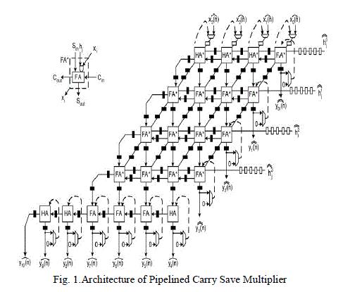 |
| Fig. 1 shows the architecture of pipelined carry save multiplier. In carry-save multipliers, carries are propagated during each additions. This carry-propagation limits the speed of multiplication. In a case involving several additions, such as partial product accumulation in multiplication. It is not strictly necessary to propagate these carries during each cycle. Instead, the carries generated during the addition of pair of operands can be saved and added, with proper alignment to the next operands. This leads to a concept of carry-save addition. In the carry-save array multiplier, the carry outputs are saved and used in the adder in the next row. In this case, the partial product is replaced by a partial sum and partial carry, which are saved and passed onto the next row. The advantage is that the addition at different bit positions in the same row are now independent of each other and can be carried out in parallel. |
| This carry-save addition can be applied to all but the last step, where there is no more multiplicand-multiple to be added, but the partial sum and partial carry. The addition of partial sum and partial carry is performed by a vector merging adder(VMA). The VMA can be implemented either as a carry save array which contains only half adders and a more regular and easier to pipelined structure. When bot level pipelining is not required, the carry-ripple and carrysave principles can also be combined into a single structure, where the carry output can ripple through at most 1 bit in the same row, and the resulting carry from each ripple portion is passed on to the next row like the carry-save architecture.[6] |
| ARCHITECTURE OF FOLDED FIR FILTER STRUCTURE |
| In Fig. 2, a folded implementation of this filter is given. It consists of an M-A unit that performs one multiplication and addition at each clock cycle. Such operations are required to produce one result at the output. The filter coefficients are stored in a cyclic shift register coefficient register (C-R) in descending order (at the right end of the register). The samples are stored in the cyclic shift register data register (D-R) in ascending order (the oldest at the left end of the register). |
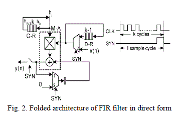 |
| The timing diagram in Fig. 2 clarifies the operation of the circuit. The computation cycle lasts clock cycles. During those cycles the most recent samples as well as the coefficients are cyclically shifted in order to compute the convolution. At the last clock of the operation cycle, when the control signal SYN is high, a new input sample enters the circuit and replaces the oldest stored input sample in D-R. At the same clock, the delay element of the accumulator is cleared while the switch at the output of the circuit closes and the final result is produced. Thus the circuit is of immediate response. The circuit operates at clock frequency. An input sample is processed every clock cycles and therefore the filter operation frequency is fs. Te frequency of the control signal SYN is .The D-R at the data input corresponds to the delay elements in the data line. The C-R corresponds to the data latches where the filter coefficients are stored when the filter is programmed. |
| FOLDED FIR FILTER SCHEME BASED ON PIPELINED CARRY SAVE MULTIPLIER |
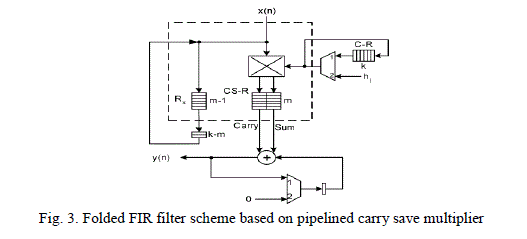 |
| The circuit, drawn in detail in Fig. 3, implements the above filter scheme for filter taps. The i-order bit of the input sample x(n), the coefficient hj and the output y(n) is represented the dashed lines represent the accumulation feedback loop. The feedback lines of x(n) and y(n) are not shown in order the complexity of the schematic to be kept low. In this example the length of Rx is equal to k-2, so one external delay for is required. The length of Rh is b=4 (less than k ), so five additional delays in each bit line of have been added on the right side of the multiplier. The external delays are represented with empty boxes and the internal delays with filled boxes. The diagonal row of cells at the right edge of the array is used for the accumulation of the least significant part of the result. For the accumulation of the most significant part, an additional row of full-adders has been added at the bottom of the array. This row is extended leftwards by full-adders to avoid accumulation overflows. The structure of the M-A unit using a pipelined carry save multiplier is shown. The pipelined carry save has internal delays, denoted within the figure, only in the bit-lines. These delays can be used for the implementation of D-R. The register for the implementation of C-R must be added externally as shown, where the implementation of a folded FIR filter in direct form is given based on the M-A unit of Fig. 3. External delays must also be added to in order to become equal to the required length for the D-R. The circuit implements the above filter scheme. The accumulation is performed by a bit-skew adder which is implemented by the diagonal line of full-adders at the right edge of the array. It is extended leftwards by full-adders, in order to avoid the accumulation overflow. The dashed lines represent the accumulation feedback loop. The external delays are represented with empty boxes. The feedback lines of and have been omitted in order to keep the complexity of the schematic low. The most significant part of the result is in carry–save form. Therefore, a triangle of delays and a row of full-adders is attached to the bottom of the multiplier, in order to convert the result in bit-skew binary form.[7] |
| FOLDING CONCEPT |
| In synthesizing DSP architectures, it is important to minimize the silicon area of the integrated circuits, which is achieved by reducing the number of functional units (such as adders and multipliers). The folding transformation is used to systematically determine the control circuits in DSP architectures where multiple algorithm operations are timemultiplexed to a single functional unit. By executing multiple algorithm operations on a single functional unit, the number of functional units in the implementation is reduced, resulting in an integrated circuit with low silicon area[2]. |
| FOLDING TRANSFORMATION |
| The folding transformations provide a systematic technique for designing control circuits for hardware where several algorithm operations are time multiplexed on a single functional unit. While folding transformation reduces the number of functional units in the architecture , it may also lead to an architecture that uses a large number of registers. To avoid architectures using excessive amount of registers, techniques can be used to compute the minimum number of registers required to implement a folded DSP architecture and to allocate data to these registers. Using register minimization technique along with folding transformation not only reduces the number of functional units but also keeps the area consumed by memory in the folded architecture to be minimum. |
V. RESULTS AND DISCUSSIONS |
| TANNER EDA |
| Tanner EDA is a leading provider of Electronic Design Automation (EDA) software solutions for the design, layout and verification of analog/Mixed Signal ICs and MEMs. This tool helps to automate and simplify the design process,enabling engineers to cost-effectively bring commercially successful electronic products to market ahead of the competition. |
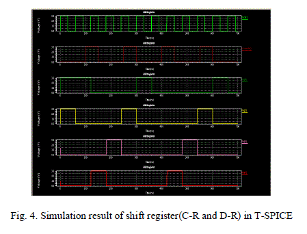 |
| Fig. 4 shows the simulation result of C-R and D-R in T-Spice. Here The filter coefficients are stored in a cyclic shift register coefficient register (C-R) in descending order (at the right end of the register). The samples of are stored in the cyclic shift register data register (D-R) in ascending order (the oldest at the left end of the register). |
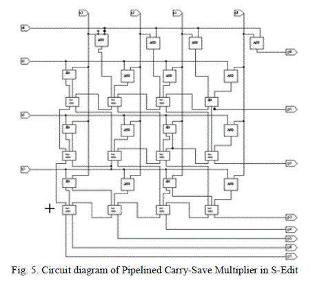 |
| Fig. 5 shows the circuit diagram of pipelined carry save multiplier in S-Edit where carries are propagated during each additions. This carry-propagation limits the speed of multiplication. In a case involving several additions, such as partial product accumulation in multiplication. In this case, the partial product is replaced by a partial sum and partial carry, which are saved and passed onto the next row. |
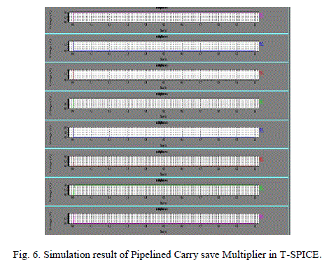 |
| In Fig. 6, the output waveform of pipelined carry save multiplier is shown. The output shows that there is small delay difference due to the logarithmic behavior of the reduction tree that reduces the benefit of a reduced number of partial product rows. |
| COMPARISON OF RESULTS |
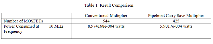 |
| From the simulation result, it is found that the power consumption for conventional multiplier and pipelined carry save multiplier and are found to be 8.974168e-004 watts and 5.9017e-004 watts. From the results, it is inferred that the pipelined carry save multiplier has reduced hardware complexity and lesser power consumption when compared with conventional multiplier. |
VII.CONCLUSION |
| The possibility of incorporating a whole signal processing system into a chip has a multitude of effects. It will dramatically increase the processing capacity and simultaneously reduce the size of the system.The paper is focused on the design of an efficient VLSI architecture for folded FIR filter which aims at reducing the hardware complexity and also to reduce the power consumption. In the proposed method, pipelined carry save multiplier is employed instead of conventional multiplier to get the better efficiency. From the simulation, it is found that the number of MOSFET’s for conventional multiplier and carry-save multiplier are 544 and 425 respectively. The power consumption for conventional multiplier and carry-save multiplier are found to be 8.974168e-004 watts and 5.9017e-004 watts From the results, it is inferred that the pipelined carry save multiplier has reduced hardware complexity and lesser power consumption when compared with conventional multiplier. Due to the lesser carry propagation, the proposed method can achieve low power consumption and higher less hardware complexity. The circuit is simulated in T-Spice in 180 nm technology. Power estimation can be obtained through transistor level design simulation. |
References |
|