International Journal of Advanced Research in Electrical, Electronics and Instrumentation Engineering
ISSN ONLINE(2278-8875) PRINT (2320-3765)
ISSN ONLINE(2278-8875) PRINT (2320-3765)
B.Madhu Latha1, B. Nageswar Rao2
|
| Related article at Pubmed, Scholar Google |
Visit for more related articles at International Journal of Advanced Research in Electrical, Electronics and Instrumentation Engineering
An 8-bit Vedic multiplier is improved in terms of transmission delay when compare with the extra predictable multipliers. We have employed 8-bit barrel shifter which craves for only one clock cycle for ‘n’ amount of shifts in our projected design. The arrangement is implemented and checked using FPGA and ISE Simulator. The central part was implemented on Xilinx Spartan-6 family xc6s1x75T-3-fgg676 FPGA. The transmission delay contrast was excerpted from the synthesis report and static timing report too. The structural design might attain propagation delay of 6.781ns by means of barrel shifter in base selection module and multiplier.
Keywords |
| Vedic multiplier; Barrel shifter; FPGA; Propagation delay; Power index. |
INTRODUCTION |
| A multiplier is one of the key hardware blocks in most of applications such as digital signal processing encryption and decryption algorithms in cryptography and in other logical computations. With forthcoming technology, many researchers tried to design multipliers which offer either of the factors high speed, low power consumption, regularity of layout and less area or even grouping of the three in multiplier. Multiplier is the core component of any DSP applications and hence speed of the processor mostly depends on multiplier design. Since multiplication dominates the execution time of most DSP algorithms, so there is a necessity of high speed multiplier. Currently, multiplication time is the dominant factor in shaping the instruction cycle time of a DSP chip. |
| Here we consider a high speed Vedic multiplier using barrel shifter. We have implemented the sutra by modified design of “Nikhilam Sutra” due to its characteristic of reducing the number of partial products. The barrel shifter is utilized at different levels of designs to lessen the delay when compared to conventional multipliers. Vedic mathematics has proved to be the most robust technique for arithmetic operations. In contradiction to conventional techniques for multiplication provide significant amount of delay in hardware implementation of n-bit multiplier. Moreover, the combinational delay of the design reduces the presentation of the multiplier. Hardware-based multiplication mostly depends upon structural design selection in FPGA or ASIC. The Sutras are helpful in saving a lot of time and lessen the effort in solving the issues, compared to the official methods presently in rage. Though the solutions appear like super natural but it is perfectly logical and rational. |
| Since, the ever mounting technology and augmented complexity in the design demands for the optimized area and delay. Researchers are persistently working on towards the designing of optimized multiplier architecture. Critical path delay is the vital factor in determining the speed of the multiplier. In simpler form multiplication can be developed using successive addition, subtraction and shifting operation as in literature. Throughput is the gauge of the number of multiplications that are performed in a given period of time. Multiplier is not only a high delay block but also a major source of power dissipation. So, if we aim to minimize power consumption, it is of great consideration to decrease the delay by using a variety of delay optimizations. |
| Digital multipliers are the core components of all the digital signal processors (DSPs) and the speed of the DSP is largely determined by the speed of its multipliers. The two most common multiplication algorithms in the digital hardware are array multiplication algorithm and Booth multiplication algorithm. The calculation time taken by the array multiplier is comparatively less because the partial products are calculated separately in parallel. The delay related with the array multiplier is the time taken by the signals to propagate through the gates that form the Multiplication array. Booth multiplication is another significant multiplication algorithm. Large booth arrays are necessary for high speed multiplication and exponential operations which sequentially need large partial sum and partial carry registers. Multiplication of two n-bit operands using a radix-4 booth recording multiplier requires approximately n / (2m) clock cycles to generate the least significant half of the concluding product, where m is the amount of Booth recorder adder stages. Thus, a large propagation delay is allied with this case. |
VEDIC MULTIPLICATION |
| The Vedic multiplier is based on the Vedic multiplication formulae (Sutras). These Sutras are used for the multiplication of two numbers in the decimal number system. Here, we apply the similar thoughts to the binary number system to build the proposed algorithm compatible with the digital hardware. Vedic multiplication based on some algorithms, Vedic Sutras are applied to and wrap up almost every branch of Mathematics. They even apply to complex problems relating a large number of mathematical operations. The Sutras are helpful in saving a lot of time and lessen the effort in solving the issues though the solutions appear like the supernatural, but it is perfectly logical and rational. The computation made on the computers follows, in a way, the principles original the Sutras. The Sutras provide not only methods of estimate, but also ways of thinking for their application. |
| Application of the Sutras improves the computational skills of the beginners in a wide area of evils, assuring both speed and accuracy, firmly depending upon normal and logical reasoning. Application of the Sutras to precise problems indulges rational thinking, which, in the process, helps get better intuition that is the outcome of the mastery of the mathematical geniuses of the past and the present namely Aryabhatta, Bhaskaracharya, Srinivasa Ramanujan, etc. |
| Multiplier implementation using FPGA previously been reported using various multiplier architectures but the concert of multiplier was better in proposed design. On the employment of Vedic multiplier which uses modified “Nikhilam Navatascaramam Dasatah” sutra. The architecture is modified using barrel shifter by which considerable amount of clock cycles are decreased by asset of that the speed increases. The presentation of the proposed multiplier is compared with the earlier implemented multipliers on FPGA. |
Nikhilam Sutra |
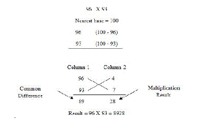
| Nikhilam Sutra factually means “all from 9 and last from 10”. Although it is valid to all cases of multiplication, it is more capable when the numbers involved are big. Since it checks out the compliment of the large number from its adjacent base to perform the multiplication operation on it, better is the original number, lesser the complexity of the multiplication. We first illustrate this Sutra by in view of the multiplication of two decimal numbers (96 * 93) where the chosen base is 100 which is nearest to and greater than both these two numbers |
 |
Multiplication Using Nikhilam Sutra |
| The right hand side (RHS) of the product can be attained by just multiplying the numbers of the Column 2 (7*4 = 28). The left hand side (LHS) of the product can be found by cross subtracting the succeeding number of Column 2 from the initial number of Column 1 or vice versa, i.e., 96 - 7 = 89 or 93 - 4 = 89. The concluding result is attained by concatenating RHS and LHS (Answer = 8928) |
| This sutra is used in this work to find the cube of a number. The number M of N bits having its cube to be calculated is divided in two partitions of N/2 bits, say a and b, and then the Anurupye Sutra is applied to locate the cube of the number. In the above algebraic explanation of the Anurupye Sutra, we have seen that a3 and b3 are to be calculated in the final computation of (a+b)3. |
PROPOSED MULTIPLIER ARCHITECTURE DESIGN |
| The 8x 8 bit multiplier is designed using 4X4 bit. A can be decomposed into pair of 4 bits AH-AL. in the same way multiplicand B can be decomposed into BH-BL. The 16 bit result can be written as: |
| P= A x B= (AH-AL) x (BH-BL) |
| P = AH x BH+AH x BL + AL x BH+ AL x BL |
| The outputs of 4X4 bit multipliers are added so as to obtain the concluding product. Thus, in the last stage two adders are also necessary. Now the basic building block of 8x8 bits Vedic multiplier is 4x4 bits multiplier which implemented in its structural model. For larger multiplier implementation like 8x8 bits multiplier the 4x4 bits multiplier units are used as components which are implemented previously in ModelSim6.1e or Xilinx ISE9.2i library. The structural modeling of any design displays fastest design. The mathematical expression for modified nikhilam sutra is given below. |
| P=X*Y= (2^k2)*(X+Z2*2^(k1-k2))+Z1*Z2 – (1) |
| Where k1, k2 are the utmost power index of input numbers X and Y respectively. |
| Z1 and Z2 are the residues in the facts X and Y correspondingly. |
| The hardware deployment of the above expression is partitioned into three blocks. |
| A. Base Selection Module |
| B. Power index Determinant Module |
| C. Multiplier |
A. BASE SELECTION MODULE |
| The base selection module has power index determinant (PID) as the sub-module together with barrel shifter, adder, normal determinant and comparator and multiplexer. An input 8-bit number is given to power index determinant (PID) to deduce utmost power of number which is fed to barrel shifter and adder. The output of the barrel shifter is ‘n’ number of shifts regarding the adder output and the input based to the shifter. At the present, the outputs of the barrel shifter are fed to the multiplexer with comparator input as a selection line. |
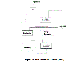 |
| Figure 1: Base Selection Module (BSM) |
| The outputs of the average determinant and the barrel shifter are fed to the comparator. The necessary base is attained in conformity with the multiplexer inputs and its corresponding selection line. |
B. POWER INDEX DETERMINANT |
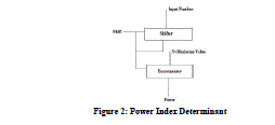 |
| Figure 2: Power Index Determinant |
| The input number is fed to the shifter which shifts the input bits by one clock cycle. The shifter pin is casted to shifter to verify whether the number is to be shifted or not. In this power index determinant (PID) the chronological searching is employed to search for initial ‘1’ in the input number starting from MSB. If the search bit is ‘0’ then the counter value will decrement up to the detection of input search bit is ‘1’. Now the output of the decrementer is the necessary power index of the input number. |
C. MULTIPLIER ARCHITECTURE |
| The base selection module and the power index determinant form integral part of multiplier design. The architecture computes the arithmetical expression in equation1.Barrel shifter used in this architecture. |
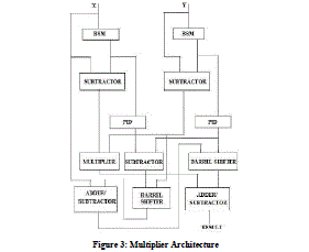 |
| The architecture implements the equation (1). Base is obtained from BSM when the numbers are provided to it. The output of BSM and the input numbers A and B are fed to the subtractors. Subtractor block provides residual part Z1 and Z2.Power Index Determinant (PID) receives values from BSM of respective input numbers. The power of the base is found by subsection of PID. The outputs of subtractor are fed to the multiplier that feeds the input to the second adder or subtractor. Similarly the outputs of PID are fed to the third subtractor that feeds the input to the barrel shifter. The input number A and the output of barrel shifter are rendered to first adder/subtractor and the output of it is applied to the second barrel shifter which will provide the in-between value. The last sub-section of this multiplier architecture is the second adder/subtractor which provides the required result. |
RESULTS |
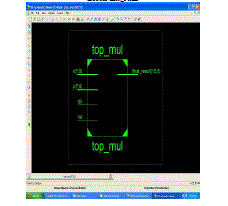
| Block diagram |
 |
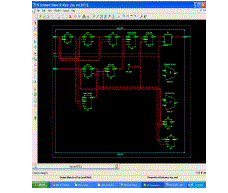
| RTL schematic |
 |
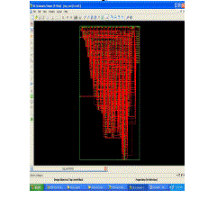
| Technology schematic |
 |
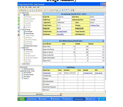
| Design summary |
 |
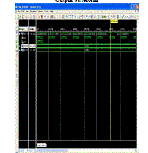
| Output waveform |
 |
CONCLUSION |
| Upon completion of the project, we achieve a high percentage of reduction in the propagation delay when compared to array multiplier and conventional Vedic multiplier implementation on FPGA. The wide ranges of applications of multiplier unit can be witnessed in VLSI and signal processing applications. The project can be extended to the power analysis of the multiplier. |
References |
|