International Journal of Advanced Research in Electrical, Electronics and Instrumentation Engineering
ISSN ONLINE(2278-8875) PRINT (2320-3765)
ISSN ONLINE(2278-8875) PRINT (2320-3765)
N. Basanta Singh
|
| Related article at Pubmed, Scholar Google |
Visit for more related articles at International Journal of Advanced Research in Electrical, Electronics and Instrumentation Engineering
Single Electron Transistor (SET) is an attractive technology for future low power VLSI/ULSI systems. SET has high integration density and ultra-low power consumption. However, Single electron transistors have extremely poor driving capabilities so that direct application to practical circuits is as yet almost impossible. An approach to overcome this problem is to build hybrid circuits of SETs and CMOS. In this work, hybrid SET-CMOS 4-to-1 MUX and 2-to-4 Decoder are designed and implemented. The MIB compact model for SET device and BSIM4.6.1 model for CMOS are used. All the circuits are verified by means of T-Spice simulation software.
Keywords |
| Single Electron Transistor, CMOS, Hybrid CMOS-SET Circuits, MIB, T-Spice, 4-to-1 MUX and 2-to-4 Decoder. |
I. INTRODUCTION |
| Single Electron Transistor is an attractive candidate for future ultra low power VLSI and ULSI systems. However, practical SET circuit applications are likely not feasible with a pure Single Electronics approach, mainly due to its low current drive. And also it is unlikely that SET can replace the CMOS technology. However, the unique properties such as Coulomb blockade oscillations of SETs can be exploited to increase CMOS functionalities by hybrid CMOS-SET approach. By combining SET and CMOS, and exploiting the Coulomb Blockade oscillation phenomenon of SET and high current drive facility of CMOS, one can bring out new functionalities which are very difficult to implement by pure CMOS approach. |
| Single electronics implies the possibility to control the movement and position of a single electron or a small amount of electrons [1]. Single-electron transistors (SETs) are three-terminal switching devices which consist of a small conducting island coupled to source and drain leads by tunnel junctions and capacitively coupled to one or more gates. The first experimental SETs were fabricated by Fulton and Dolan [2] and Kuzmin and Likharev [3] in 1987. SET is expected to be a key device for future VLSI/ULSI circuit implementation because of its low power dissipation, small size and highly functional features [1, 4]. The real problems preventing the use of SETs in most applications are their low current drivability, small voltage gain, high output impedance, and high sensitivity to background charges [5-9]. Since CMOS devices have advantages that can compensate for the drawbacks of SETs, hybrid SET-CMOS circuits that combine both SET and CMOS devices is one of the possible solutions to the problems of SET mentioned above. |
| In this work, hybrid SET-CMOS 4-to-1 MUX and 2-to-4 Decoder circuits are designed and implemented. The operation of the proposed circuits are analyzed and verified in Tanner environment. The MIB compact model for SET devices and BSIM4.6.1 model for CMOS are used. |
II. THEORY |
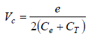
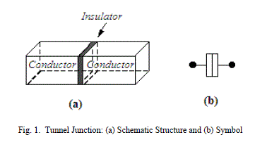
| The main device of the Single Electron technology is the tunnel junction through which individual electron can move in a controlled manner [10]. Their operation is based on the Coulomb blockade [11]. A schematic structure and symbol of a tunnel junction are shown in Fig. 1. It can be considered as two conductors separated by a thin layer of insulating material. Electrons are considered to tunnel through a tunnel junction one after another [12- 14]. The required threshold voltage across the tunnel junction to make a tunnel event possible, known as known as the critical voltage Vc, can be calculated with the equation [13] |
 (1) (1) |
| Where e = 1.602 x 10⁻¹⁹ C, CT is the junction capacitance and Ce is the equivalent capacitance for remainder circuit as viewed from the tunnel junctionâÃâ¬ÃŸs perspective. |
 |
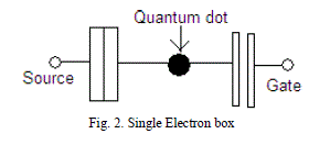
| The simplest functional single-electron device is a single-electron box [3]. The equivalent circuit of a single-electron box is shown in Fig 2. It is composed of a quantum dot connected with two electrodes. One electrode, called the source electrode, is connected with the quantum dot through a tunnel junction and the other electrode, called the gate electrode, is coupled with the quantum dot through a thicker insulator which does not allow noticeable tunnelling [3]. Therefore, electrons are injected into or ejected from the island through the tunnel junction. The number of electrons in the island can be controlled by using the gate electrode. Although a single-electron box can control the number of electrons in the island, it does not have the properties of a switching device which are essential elements of VLSI/ULSI circuits. |
 |
2.1 SINGLE ELECTRON TRANSISTOR (SET) |
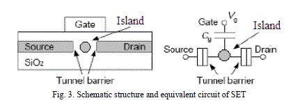
| Single electron transistors are three-terminal switching devices. A schematic structure and equivalent circuit of an SET are shown in Fig. 3. The two tunnel junctions create a "Coulomb island or Quantum dot" that electrons can only enter by tunnelling through one of the tunnel junctions. The gate terminal is capacitively coupled to the node between the two tunnel junctions. The capacitor may seem like a third tunnel junction, but it is much thicker than the others so that no electrons can tunnel through it. The capacitor simply serves as a way of setting the electric charge on the coulomb island. |
 |
| SET can transfer electrons form source to drain one by one and therefore can be used as a switching device. Electrons have to tunnel through the junction from the source to the drain via the central island for normal operation of the SET. For tunnelling to happen, the charging energy EC should be greater than the thermal energy and also the tunnelling resistance RT should be greater than the resistance quantum h/e2. Therefore the conditions for observing single-electron phenomenon is |
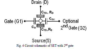
| expressed as Ec e 2C KBT 2 and 2 RT h e where C is the total island capacitance with respect to the ground, KB is the BoltzmannâÃâ¬ÃŸs constant, T is the temperature and h is the PlanckâÃâ¬ÃŸs constant. SETs may also have an optional 2nd gate connected to the island that can be used for controlling the phase shift of coulomb oscillation. The circuit schematic of such an SET is shown in Fig 4. In Fig 4, CTD is the drain tunnel junction capacitance, CTS is the source tunnel junction capacitance, RD is the drain tunnel junction resistance, RS is the source tunnel junction resistance, CG is the gate capacitance and CG2 is the optional 2nd gate capacitance. |
 |
2.2 MIB MODEL OF SET |
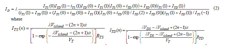
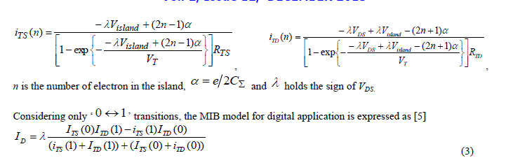
| The MIB model is a physically based compact analytical model for SET [5]. The model is based on the assumptions that it obeys the orthodox theory of single-electron tunnelling and the interconnect capacitances associated with the source, drain and gate are much larger than the device capacitance so that the total capacitance of the island with respect to ground will be equal to the summation of all device capacitances i.e C CTD CTS CG1 CG2 . Not all tunnelling current components are equally important and keeping only important tunnelling components of the current, the drain current in the MIB model for analog application is expressed as [5] |
 |
 |
III. HYBRID SET-CMOS LOGIC GATES |
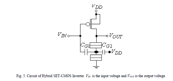
| The circuit of a Hybrid SET-CMOS Inverter proposed in Ref. 15, which is formed by a PMOS transistor as the load resistance of an SET is shown in Fig 5. Although it resembles a CMOS inverter, there are two differences [15]: |
| (a) The pull down transistor is an SET and |
| (b) VDD is defined by the SET device parameters |
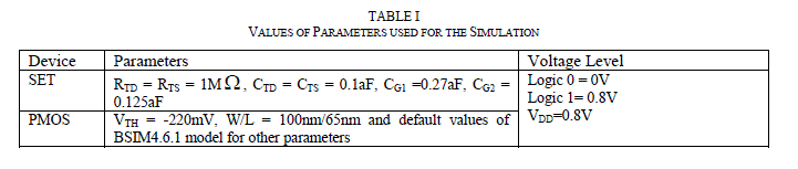
| Since the MIB model is valid for V e C DD 3 [7] for single/multiple gate(s) and symmetric or asymmetric SET devices, the bias voltage is taken as 800mV. The values of the tunnel junction capacitors (CTD and CTS) have been designed to prevent tunnelling due to thermal energy. The values of the parameters used for the devices are given in Table I. |
 |
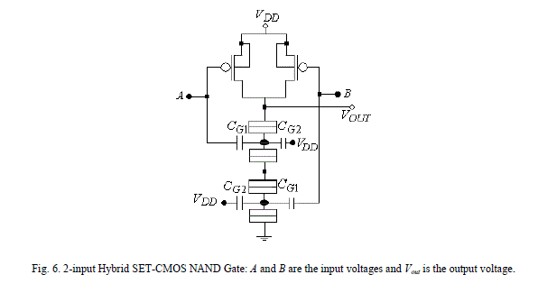
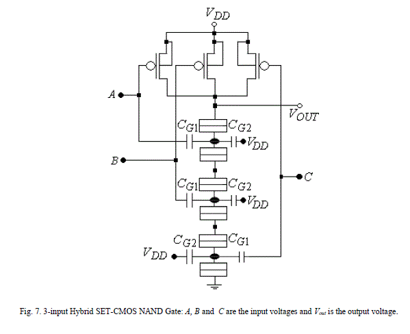
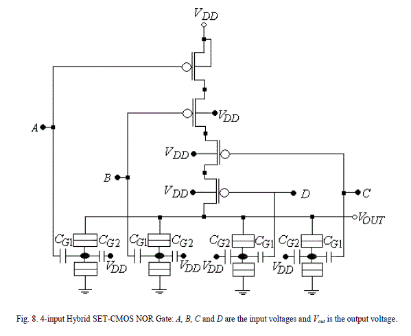
| Based on the idea that serial connection is AND and parallel connection is OR, the circuits of 2-input NAND, 3-input NAND and 4-input NOR are realized using the hybrid CMOS-SET inverter. The circuits of 2-input NAND, 3-input NAND and 4-input NOR are shown in Figs 6-8. The circuits of AND and OR can be realized by connecting an inverter at the output of NAND and NOR. |
 |
 |
 |
IV. DESIGN OF HYBRID SET-CMOS 4-TO-1 MUX AND 2-TO-4 DECODER CIRCUITS |
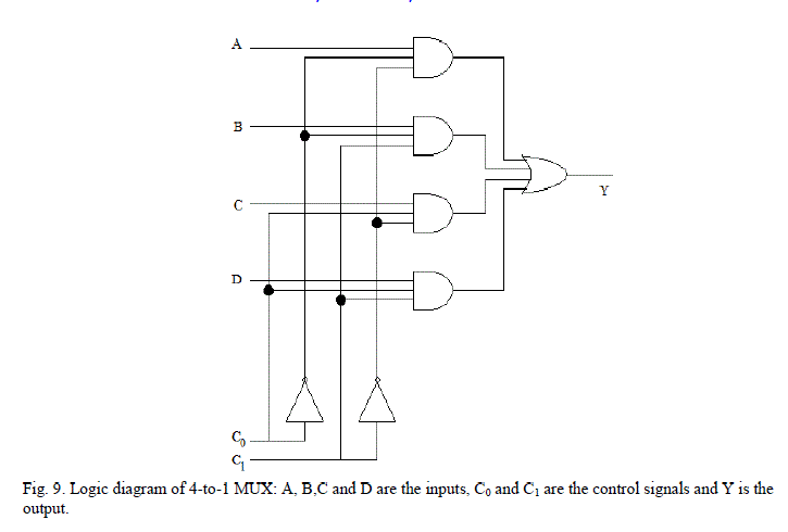
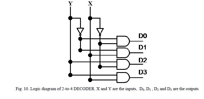
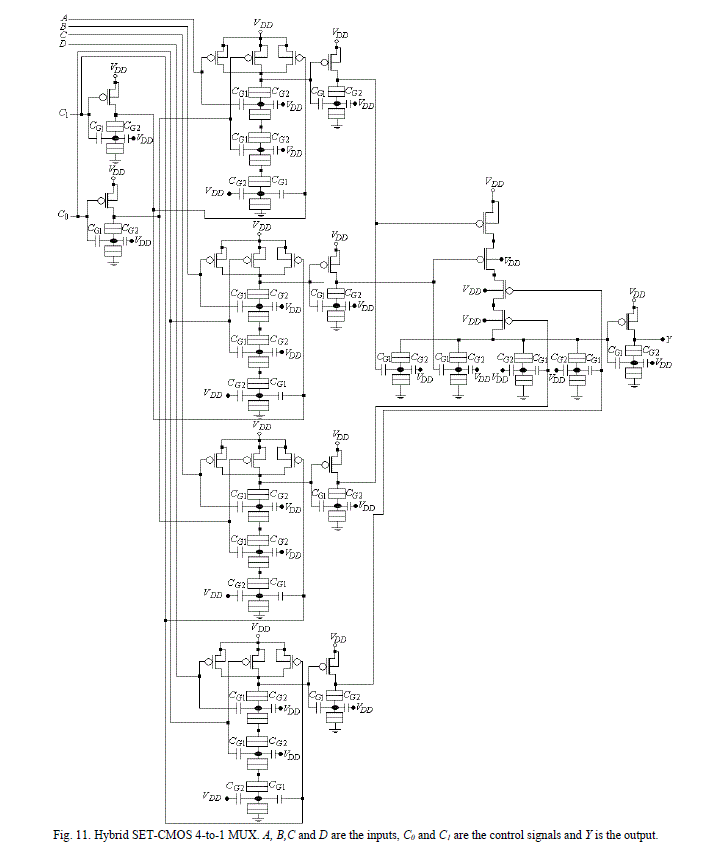
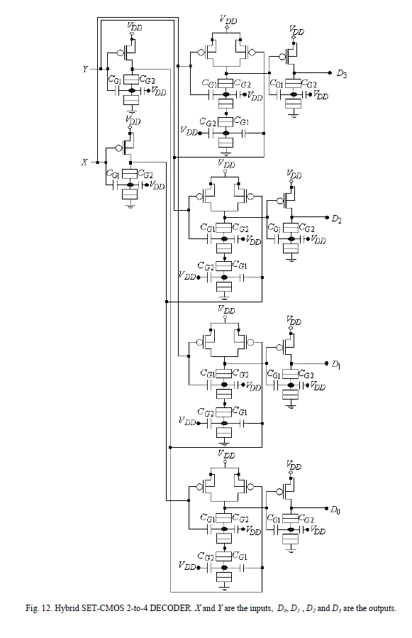
| The logic circuits for 4-to-1 MUX and 2-to-4 Decoder are shown in Figures 9 and 10. The design is done following conventional digital system design scheme and hence not detailed here. Using the structure of their CMOS counterparts, the circuits of 4-to-1 MUX and 2-to-4 Decoder implemented using the hybrid SET-CMOS logic gates are shown in Figures 11 and 12, respectively. |
 |
 |
 |
 |
V. RESULTS AND DISCUSSION |
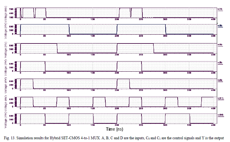
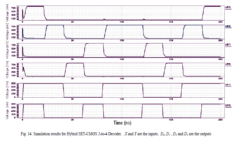
| The proposed circuits are simulated using the MIB compact model described by Analog Hardware Description Language (AHDL) for SET and BSIM4.6.1 model for MOSFET in Tanner environment. The values of the parameters used for our simulation are given in Table I. The simulation result of Hybrid SET-CMOS 4-to-1 MUX is shown in Fig 13. A, B, C and D are the inputs, C0 and C1 are the control signals and Y is the output. The simulation result of Hybrid SET-CMOS 2-to-4 Decoder is shown in Fig 14. X and Y are the inputs, D0, D1 , D2 and D3 are the outputs. From Figs 13 and 14, it can be easily verified that the performances of Hybrid 4-to-1 MUX and 2-to-4 Decoder are satisfactory. |
 |
 |
 |
VI. CONCLUSION |
| The design and simulation of hybrid SET-CMOS 4-to-1 MUX and 2-to-4 Decoder are presented. The performances of the proposed circuits are verified by simulation using T-Spice simulation software. The simulation results show that the performances of the circuits presented in this paper are satisfactory thereby establishing the feasibility of using the proposed hybrid circuits in future low power ultra-dense VLSI/ULSI circuits. |
References |
|