International Journal of Advanced Research in Electrical, Electronics and Instrumentation Engineering
ISSN ONLINE(2278-8875) PRINT (2320-3765)
ISSN ONLINE(2278-8875) PRINT (2320-3765)
Rajlaxmi Belavadi1, Pramod Kumar.T1, Obaleppa. R. Dasar2, Narmada. S2, Rajani. H. P3
|
| Related article at Pubmed, Scholar Google |
Visit for more related articles at International Journal of Advanced Research in Electrical, Electronics and Instrumentation Engineering
This paper explores the design and analysis of Static random Access Memory (SRAMs), focusing on optimizing delay and power. To address sub threshold leakage issue full stack approach is used. The full stack technique reduces leakage power to a great extent. The full stack technique is applied to SRAM cell in asymmetric manner in order to realise still higher power reduction. This work compares performance of SRAM using full stack approach with that of conventional 6T-SRAM design. The impact of temperature and different process corners on the performance of full stack design is also analysed. The static power and dynamic power measurement is done using Cadence Virtuoso ADE Visualization and Analysis XL Browser and XL Calculator. The layout is drawn and verified for DRC, LVS and RC extraction using Cadence Assura Tool.
Keywords |
| 10T SRAM, Full Stack, Dual Vth, Low Power. |
I. INTRODUCTION |
| SRAM is a type of semiconductor memory which does not need to be periodically refreshed. With scaling down of technology, the feature sizes have shrunk more and more and miniaturization at chip level has occurred. But as a trade off, the demand for power has also increased. SRAM continues to be a critical component in microelectronics applications. Leakage is a serious problem particularly for SRAM. With shrinking technologies the threshold voltage is decreasing and leakage current of SRAM is increasing. |
| SRAMs contribute to a significant portion of the total system power dissipation. Caches, tag arrays, register files, branch table predictors, instruction windows, translation look aside buffers are common examples of microprocessor modules in which SRAMs are used. For the CMOS feature sizes below 180nm, leakage power dissipation has become an overriding concern for VLSI circuit designers. Power consumption of CMOS consists of dynamic and static components. Dynamic power is consumed when transistors are switching, and static power is consumed regardless of transistor switching [1]. |
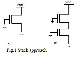
| Since cache memory cells remain in idle state most of the time static power is becoming an overriding concern in submicron technologies. This work focuses on static power reduction using stack principle. Fig.1 shows the structure of stack approach. When the two transistors are turned off together, induced reverse bias between the two transistors results in sub-threshold leakage current reduction. However, divided transistors increase delay significantly and could limit the usefulness of the approach [2]. In Fig.1 single transistor is divided into two transistors. The stack effect occurs when two or more stacked transistors are turned off together; the result is reduced leakage power consumption. The leakage through two series OFF transistor is much lower than that of a single transistor because of the stack effect. |
 |
II. MEMORY ARCHITECTURE |
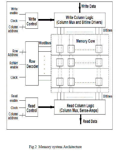
| Fig.2 shows a typical structure of Memory architecture [3]. It is primarily composed of the following sub-blocks: address decode logic, memory core, read column logic, write column logic, read control, and write control logic. While the generic structure of SRAMs is usually the same, SRAMs typically differ from each other in their size, organization of the memory core (in terms of number of rows and columns). SRAMs usually support read and write operations [6]. For these operations, the row decoder selects the appropriate wordline corresponding to the input address thereby activating a row in the memory array. |
| For a read operation, the precharged bitlines either retain charge or discharge depending on the data stored in the memory core cells selected by the wordline. The sense-amplifier in the read logic detects the changes in the voltage on the bitlines and the appropriate data is multiplexed to the data output. The read control logic controls the signals to the sense-amplifiers and bitline precharge logic [3]. |
| For a write operation, the sense-amplifiers are isolated and the write buffers in write logic drive the bitlines in accordance with the data to be written into the memory location corresponding to the write address. After a read/write has been performed, the bitlines are precharged to supply voltage (referred to as precharge phase) thereby getting ready for another read/write in the next cycle. Typically, in a SRAM clock cycle, while read/write is performed in the first phase (referred to as read/write phase) of the clock cycle, precharge is performed in the second phase. Bitline precharge is done independent of the operation in the first phase of the clock cycle. If there is no operation being performed in a clock cycle, all the wordlines remain deactivated (logic LOW) and the bitlines stay precharged (logic HIGH). This no operation phase is referred as idle phase. The leakage current in SRAMs vary within a clock cycle depending on the phase of the operation being performed, since different transistors would be in off state during different operations[3]. |
 |
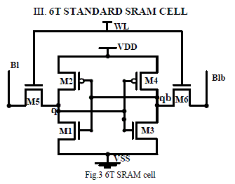 |
| Data 0 or 1 is stored in SRAM cell, using two cross coupled inverters. This storage cell has two stable states 0 and 1 which is reinforced because of cross coupling. Two additional access transistors serve to control the access to the storage cell during read and write operations. So a typical SRAM cell is a six transistor structure. A 6T SRAM cell requires a careful device sizing to ensure read stability, write margin and data retention in standby modes. The Fig.3 shows a typical 6T SRAM cell. Access to the cell is enabled by the word line which controls the two access transistors M5 and M6. These device inturn controls whether the cell should be connected to the bit lines. Bit lines are used for both read and write operations. For read stability, M1 transistor is required to be much larger than M5 transistor to make sure that the node between M1 and M5 does not flip. During write operation, bit lines overpower cell with a new value. High bit lines must not overpower inverters during read operation. So, M2 is designed to be weaker than M5 [4]. |
IV. MEMORY SYSTEM USING FULL STACK 10T SRAM CELLS |
| A. FULL STACK 10T SRAM CELL: |
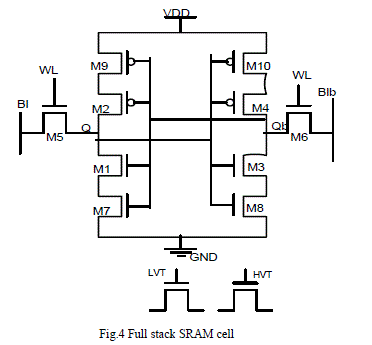 |
| The transistors M1 to M6 constitute the standard 6T SRAM cell. Stacking is applied to this cell both in the pull down and pull up section. Transistors M7 and M8 are connected as Nmos stacking transistors to pull down transistors M1 and M3.Pmos stacking transistors M9 and M10 are connected to pull up load transistors M2 and M4. During cell inactive state, the node at „0âÃâ¬ÃŸvalue is connected to ground through two series connected off transistors. This reduces leakage current due to stack effect. Similarly the leakage current flowing through off transistors in the pull up path also gets reduced due to stacking. The node storing „1âÃâ¬ÃŸgets charged by larger resistance which reduces active current and active power consumption. The power can be further lowered by using high Vt transistors. |
| In this cell both high-Vt and normal-Vt transistors are used. So that optimized delay and power can be observed. Transistor sizing for SRAM can be approached in two ways. For the function of SRAM cell, read & write stability needs to be guaranteed. In read stability, M1 transistor is required to be much larger than M5 transistor to make sure that node between M1 and M5 transistors must not flip. When in write mode, bit lines (Bl or Blb) overpower cell with new value. However, high bit lines must not overpower inverters during read operation. That results in the determination of sizing M2 transistor weaker than M5 transistor. The stacking transistors are taken as minimum size transistors [5]. |
| B. PERIPHERAL CIRCUITS |
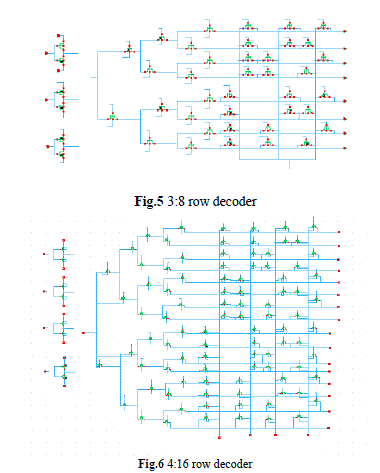
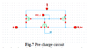
| a) Address decoding: The 8x8 SRAM system has storage capacity of 8words of 8bit each. To address these words, 3:8 row decoder is used. And for 16x16 SRAM system, 4:16 row decoders are used. Lyon-Schediwy decoder [6] which uses lesser number of transistors than the regular AND/NAND decoder is used for address generation. Since Lyon-Schediwy decoder is a faster decoder, and uses lesser number of transistors compare to regular decoder, the power dissipation is greatly reduced. The 3:8 row decoder is shown in Fig.5 and Fig.6 depicts 4:16 decoder. |
 |
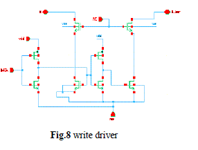
| b) Precharging: The function of the pre charge circuit is to charge the bit lines and inverse bit-lines. The precharge enables the bit-lines to be charged high at all times except during write and read cycle. Whenever the precharge signal PRE_C is applied to the equalizing transistors, it simply equalizes the voltage levels on B and B_bar [7]. |
 |
| c) Data Write Operation: The write circuit writes the data from the port and on getting the write enable signal, performs the write operation. Each of the 8 columns of the memory array has one data write circuit as shown in fig. 4. The data write circuit consists of two inverters and an AND gate implemented by pass-transistors. The data write circuitry writes data and its complement onto the bit-lines when activated by write-enable (WE) signal. The data and its complement are written onto the individual nodes Q and QN of the selected word through the access transistors of the SRAM cell. |
 |
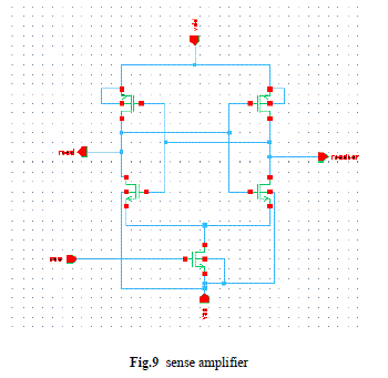
| d) Data Read Operation: The data written into the SRAM cell is retained as long as the power is present. During read operation the sense amplifier enable (SAE) signal is applied to the sense amplifier as shown in fig. 9. This activates the sense amplifier for read operation only for Short sense duration. At the same time the column is isolated from the bit-lines by using signal Ymux. This causes one of the bit-lines Bl/Blb to discharge from the precharged value. This creates a differential voltage on the bit-lines which is sensed by the sense amplifier and amplified to the full extent. The data and its complement are reflected on the output lines READ and READ_BAR[7]. |
 |
| C. LOW POWER MEMORY SYSTEM FOR ARRAYS |
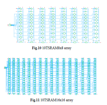
| Combining 64-10T SRAM cells, address decoder the precharge circuitry, data write circuitry, and sense amplifiers, 8x8 SRAM array is designed in 90nm CMOS technology files. Similarly 16x16 SRAM array also designed using 256-10T SRAM cells and appropriate peripheral circuitry. The complete setup is data write and read for memory array system is shown in Fig.10. This block diagram shows all the different peripheral circuits combined with the static RAM cells, to form a complete working SRAM 8 x 8 array for write and read operation. Fig.10 shows the block diagram of SRAM memory with all input signals; precharge, write enable, sense amplifier enable, 16 word lines and 16 input data bits. SRAM 16x16 array is shown in Fig.11. |
 |
V. SIMULATION AND RESULTS |
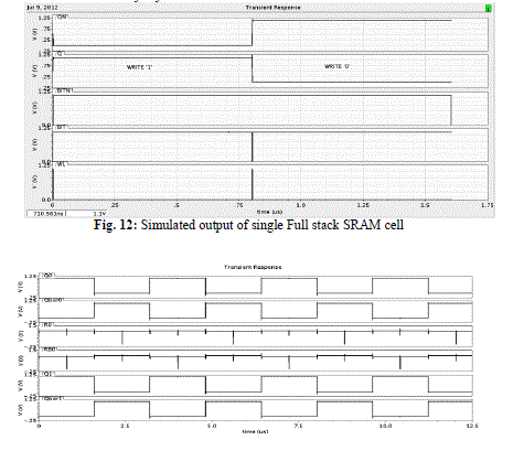
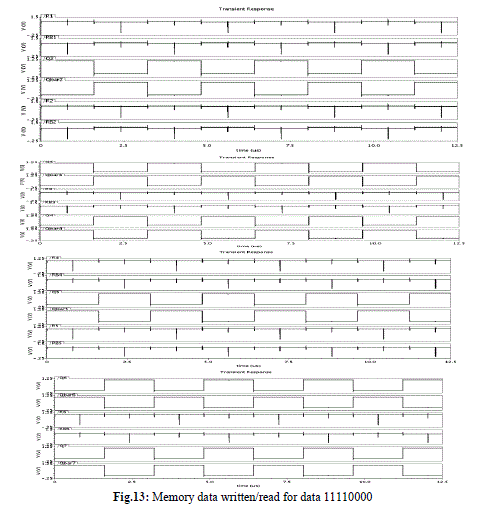
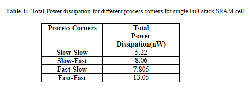
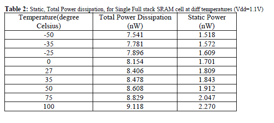
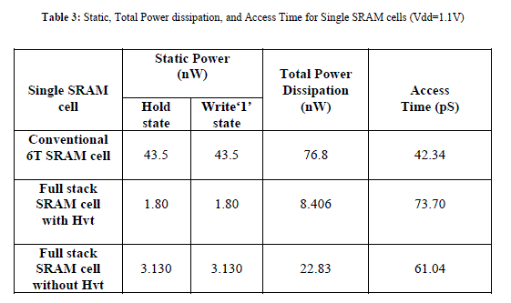
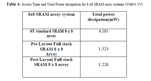
| All simulations were done in Cadence design environment, using GPDK 90nm technology files. Power dissipation is calculated across the different process corners. As the temperature increases power dissipation also increases and different temperature values are taken with a power supply voltage of 1.1V. Static power dissipation is measured during write „1âÃâ¬ÃŸ and write „0âÃâ¬ÃŸ operations as well as during cell inactive state. When compared to the total power dissipation of single 6T standard SRAM cell, it is observed that the single Full stack SRAM cell total power reduced by 9.5X times. A comparison of the Access Time, Static and Total Power Dissipation in the Full stack SRAM cell with 6T standard SRAM cell is presented in Table. 3. For 8 x 8 SRAM Array System, the Total Power Dissipation, when compared to 8 x 8 6T standard SRAM array system, it is observed that the total power dissipation of Full stack SRAM 8 x 8 array system has reduced considerably by 6X. |
 |
 |
 |
 |
 |
 |
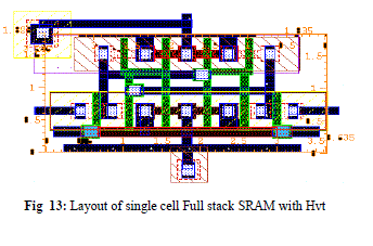
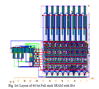
| The layout was drawn and verified for DRC, LVS and RC extraction using Cadence Assura Tool. Having successfully made layout of single bit Full stack SRAM, layout for 8 x 8 memory system of size 8words x 8bits including all the memory cells and peripherals circuits is made using Cadence Assura tool. Pre layout and Post layout Access Time, Read Time and Total Power dissipation are measured and tabulated in Table 4. |
VI. LAYOUT |
 |
 |
VII. CONCLUSION |
| In this work leakage power is reduced, at the expense of additional stacking transistors. Using full stack approach SRAM performance improved without losing read and write ability. The design and implementation of the SRAM memory done in cadence environment in 90nm process technology. The full stacking has reduced power considerably. |
References |
|