International Journal of Advanced Research in Electrical, Electronics and Instrumentation Engineering
ISSN ONLINE(2278-8875) PRINT (2320-3765)
ISSN ONLINE(2278-8875) PRINT (2320-3765)
S.Chithra1, V. Devi Maheswaran2
|
| Related article at Pubmed, Scholar Google |
Visit for more related articles at International Journal of Advanced Research in Electrical, Electronics and Instrumentation Engineering
Several techniques are available for implementing DC-DC converters using digital controllers Among these FPGA (Field Programmable Gate Array) based implementation provides various advantages in terms of speed, flexibility, low power usage, reduced equipment sizing and massive parallelism. The traditional methods allow fault diagnosis only after the final implementation which leads to extra cost and loss of design time. This paper proposes a smart method of FPGA based implementation of DC-DC Buck Boost converter control system using Matlab and ModelSim. The control algorithm and coding is done by means of Verilog code and implemented on an Altera FPGA Board. The FPGA takes control of the entire system and decides whether to increase or decrease the voltage depending on the application. Load is applied and the efficiency is checked at variable load conditions.
Keywords |
| Converters, DSP, Field Programmable Gate Arrays,Matlab, Modelsim. |
I.INTRODUCTION |
| All battery powered electronic devices have their voltage range that is in between the range of a fully charged to a semi charged battery. Since the required output may be greater or lesser than the supplied voltage, a buck and boost converter needs to be cascaded to be used for this purpose. Cascading of the two converters results in what is called as the buck-boost converter. |
| The control of these converters has been traditionally implemented using analog methodologies. But due to recent advancements of digital technology, digital controllers haven begun to replace analogue controllers. Digital systems controlled using microcontrollers and Digital Signal Processor (DSP) is being replaced by a more suitable candidate, the Field Programmable Gate Array (FPGA) [1]. A Field Programmable Gate Array (FPGA) consists of a matrix of reconfigurable gate array logic circuitry that can be configured in a way depending on the user requirement. These logic blocks when configured and connected create a hardware implementation of a software application [2]. The behaviour of FPGA can be described using a Hardware Description Language (HDL) or a schematic. The FPGA technology is now considered by an increasing number of designers in various fields of application such as telecommunication, video, signal processing, embedded control systems and electrical control systems [2]. Therefore FPGA based controller is preferable because of the following advantages [5-9]. |
| FPGA can process information faster. |
| Controller architecture can be optimized for space or speed. |
| Available in radiation tolerant package. |
| Implementation in HDL allows the targeting of a variety of commercially available device. |
| FPGA allows for implementation of parallel processing. |
| Rest of the paper is organized as follows: Section II explains the system model of buck and boost converters and their working principle. Circuit diagram of the buck boost converter is given in section III. Design equations of the converter are given in section IV. Design specifications are given in section V. Simulation results are presented in section VI. Finally conclusion is presented in chapter VII. |
II.SYSTEM MODEL |
| Fig.1 illustrates the model of the proposed buck-boost converter. The proposed system can operate in buck, boost and buck-boost modes |
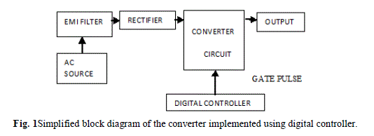 |
| The operation of the above system is as follows. A 230V/50Hz AC acts as the source of supply. This AC voltage is stepped down, rectified and regulated to obtain the desired DC input. This DC voltage is given to the buck boost converter section which converts this input value to another level of output DC voltage. The main part of the entire system is the digital controller part which issues control signals to the switch converter to the desired value. The digital controller consists of the three main parts: an Analog to Digital Converter (ADC), Pulse Width Modulator (PWM) and a compensator. Fig. 2 shows the detailed block description of the digital controller section. |
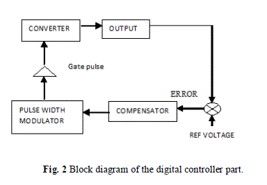 |
| The output obtained from the converter is an analog DC voltage. The analog voltage needs to be converted to its digital equivalent since the PWM can accept only digital values. This digital value is compared to a reference value and the difference is generated as an error signal that is compensated using suitable compensation methods such as PID. The compensated value is given to the Pulse Width Modulator (PWM) ,that adjusts its duty cycle according to the control signal obtained. The system can operate in three modes: |
| A. Buck mode of operation |
| The system operates in buck mode when the required voltage is less than the input voltage. The circuit is controlled with buck PWM pulses. This mode is similar to a DC-DC step down converter. |
| B. Boost mode of operation. |
| The circuit operates in boost mode when the required voltage is greater than the input voltage. The system is controlled by the boost PWM pulses generated by the FPGA. In this mode the system is similar to a DC-DC step up converter. |
| C. Combination of Buck and Boost modes. |
| When the required voltage level is close to the output voltage level, where both the buck and boost modes can’t serve the purpose the circuit operates as a combination of buck and boost modes. During this mode the system is controlled with both buck and boost PWM pulses respectively. |
III.CIRCUIT DIAGRAM OF BUCK BOOST CONVERTER |
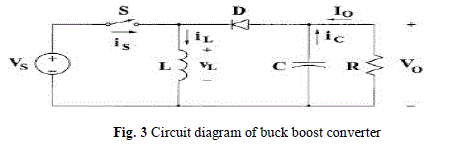 |
| The working principle of the circuit is as follows: while in the on-state, the input voltage source is directly connected to the inductor (L). This results in accumulating energy in L. In this stage, the capacitor supplies energy to the output load, while in the off-state, the inductor is connected to the output load and capacitor, so energy is transferred from L to C and R. The operation of the switch is controlled by the PWM pulses from the FPGA. |
| The output voltage is compared to a reference voltage, if they obtained voltage is lesser than the required voltage then boost PWM pulses are generated by the FPGA. If the obtained voltage is greater than the required voltage then buck PWM pulses are generated by the FPGA. |
IV.DESIGN EQUATIONS |
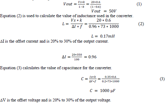
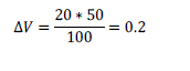
| The source voltage VS = 20V, k is the gain and should be greater than 0.5. Let the value of k be 0.6.Equation (1) helps to calculate the output voltage. |
 |
 |
V. DESIGN SPECIFICATIONS OF THE CONVERTER |
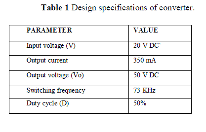 |
| As per the specifications with an input voltage of 20V with 50% duty cycle the mean output voltage obtained is between 50.77V and 50.8125V. |
VI.SIMULATION RESULTS |
| The simulation results are obtained individually for the buck boost converter section and PWM pulse generation. The main challenge lies in co-simulating Matlab and Modelsim. For the link to work, ModelSim has to be invoked from the command prompt of Matlab. |
| A. Buck Boost Converter section |
| The buck boost converter is implemented in Matlab Simulink. The simulink model is shown in fig 4. |
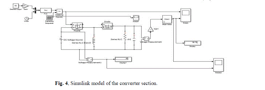 |
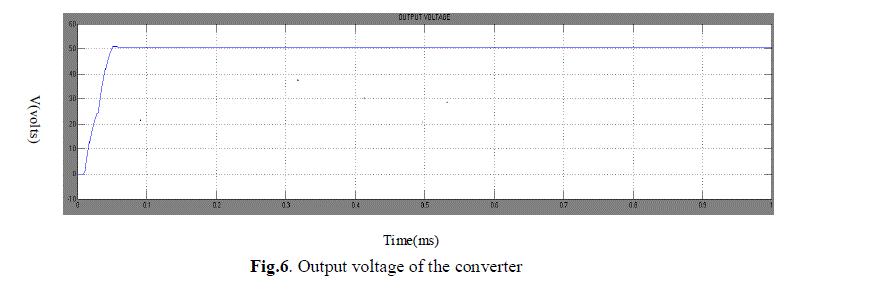
| Input voltage is obtained using a step down transformer. The 230 V AC is stepped down and rectified and an input of 20V DC is given to the buck boost converter. The PWM pulses of 50% duty cycle are given using the repeating sequence block from the Simulink library. The output voltage obtained is approximately 50 V DC. |
 |
 |
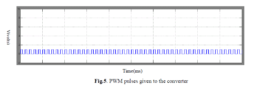
| B PWM Pulse generation for Digital Controller |
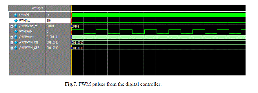
| The PWM pulses are generated using the ModelSim simulation software. The coding is done using Verilog hardware description language. The duty cycle of the pulse can be varied from 30% to 70%. Fig 7 shows the PWM pulses with 50% duty cycle. |
 |
VII.CONCLUSION |
| Thus the simulation of the DC-DC buck boost converter using the digital controller was performed and the various outputs were obtained. The digital control involved three modules; Analog to Digital Conversion (ADC), design of compensator and generation of PWM pulses. The control circuit drives the gate of MOSFET in the buck boost converter. This reduces the losses and efficiency of the converter is improved and is achieved through suitable switching process of the circuits. Such a digital control increases the speed of conversion. |
References |
|