International Journal of Advanced Research in Electrical, Electronics and Instrumentation Engineering
ISSN ONLINE(2278-8875) PRINT (2320-3765)
ISSN ONLINE(2278-8875) PRINT (2320-3765)
MadivalappaTalakal1, G.Jyothi2, K.N.Muralidhara3, M.Z.Kurian4
|
| Related article at Pubmed, Scholar Google |
Visit for more related articles at International Journal of Advanced Research in Electrical, Electronics and Instrumentation Engineering
The IEEE 754 single precision floating point multiplier uses reversible exponent adder to accomplish multiplication operation. The REA is designed and implemented using reversible logic gates like Peres gate and TR gate. Reversible logic is used to reduce the power dissipation compared to classical logic and it can also reduces the information loss so which finds application in different fields like low power computing operations, quantum computing, optical computing techniques, and may also used in other emerging computing technologies. Verilog is used to implement a technology-independent pipelined design. The multiplier can be designed to handles the overflow and underflow cases. Implementation of rounding will not gives more precision when using the multiplier in a Multiply and Accumulate (MAC) unit. In other (truncated) multiplication technique by truncation method rounding may also be implemented for further reduction in power dissipation and area. The entire design of reversible exponent addition using reversible ripple carry adder and reversible ripple borrow subtractor is modeled using Verilog hardware description language .The coding is done on Xilinx ISE 12.2 and simulation is performed on Modelsim 6.3.
Keywords |
| Floating point, Reversible logic gates, REA, Quantum computing, MAC, Truncation. |
I.INTRODUCTION |
| In the recent years reversible logic has received great attention due to their ability to reduce the power dissipation. The reduction in the power dissipation is the main requirement in low power VLSI design. Reversible logic has wide range of applications in low power CMOS technology and information processing in optical communication, DNA computing in medical field and other emerging technologies like quantum computation and nanotechnology. Irreversible (classical) hardware computation results more energy dissipation due to the loss of information bit. According to R.Landauer’s research, the amount of energy dissipated or heat generated for every irreversible bit operation is at least kTln2 joules, where k is the Boltzmann’s constant and T is the temperature at which operation is performed. The energy dissipated due to the one bit of information loss is very small at room temperature but when the number of bits is more as in the case of high speed computational operations the heat dissipated by such operation will be so large that it affects the entire performance and results in the reduction of lifetime of the components. In 1973, Bennett showed that kTln2 of energy dissipation can be reduced or eliminated from the system as long as the system allows the reproduction of the inputs from observed outputs. Due to the reproduction of inputs from outputs, reversible logic supports the process of running the system both forward and backward direction. So the reversible computations can generates inputs from outputs and can stop and also go back to any point in the computation history. A circuit is said to be reversible then its input vector can be uniquely recovered from its output vector and there is a one-to-one correspondence (mapping) between its input and output assignments, i.e. the outputs can be uniquely determined from the inputs and vice-versa. Heat generation due to information loss can be reduced or even eliminated if computation becomes lossless. |
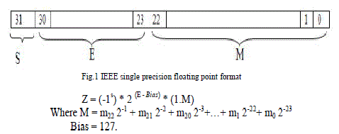
| Reversible logic gate has k inputs, and k outputs, then we call it a k X k reversible logic gate. To make the number of inputs and outputs equal additional outputs are added but which are not used in the synthesis of a given function but to achieve reversibility they are mandatorily used such outputs are called garbage. The major design constraints of reversible logic circuits are reversible logic gates do not allow fan-outs, reversible logic circuits should maintain minimum quantum cost, the compaction or optimization of design can be achieved by making the design to produce minimum number of garbage outputs and they must use minimum number of constant inputs. Floating point numbers are one possible way of representing real numbers in binary format. Two different floating point formats available in IEEE-754 standard are, Binary interchange format and Decimal interchange format. Multiplication of floating point numbers is a critical requirement for complex application like DSP applications involving large dynamic range. The implementation focuses only on the single precision normalized binary interchange format. Figure 1 shows the representation of IEEE 754 single precision binary format. It consists of a one sign bit(S), an exponent part of eight bit (E), and a Twenty three bit of fraction (M or Mantissa).To form the significand an extra bit is added to the fraction. If the exponent is smaller than 255 and greater than 0, and there is 1 in the MSB of the significand then the number is said to be a normalized, in this case the real number is represented by (1) |
 |
| Multiplication of two numbers in floating point format is done in three important steps: |
| Adding the exponent of the two numbers then bias is subtracted from their result. |
| Multiplying the significand of the two numbers. |
| Finally calculate the sign by XORing the sign of the two numbers. In order to represent the multiplication result in the form of normalized number there should be 1 in the MSB of the result (leading one). |
II.RELATED WORK |
| A number of works have been reported in the literature with an aim to achieve a reduced latency of floating –point operations. Survey on different techniques as well as components is systematically reported bellow. |
| Landauer [1] determined that the amount of energy dissipated or heat generated to erase each bit of information is at least kTln2 (where k is the Boltzmann constant i.e. 3x10¹² joule at room temperature) during any computation due to the intermediate bits. |
| C. H. Bennett [2] in 1973 proposed that the power dissipation or heat generation in any device can be made zero or less if the computation is done using reversible logic model. By considering all the concepts mentioned above the research on the reversibility was started in the year of 1980. |
| In the year 1994 Shor [3] proposed his remarkable research work in creating an algorithm using reversibility for factorizing larger number with better efficiency. After this the work on reversible computing was started by more people in different fields like low power CMOS VLSI and so on. Based on the concept of reversibility Edward Fredkin and TommasoToffoli [4, 5] introduced new reversible logic gates known as Fredkin and Toffoli reversible logic gates. These gates are used as universal gates in the reversible logic based circuits. These are the 3x3 reversible logic gates. Peres [6] also invented a new gate known as pares gate. It is a 3x3 reversible logic gate. Even though this gate is not universal gate it is widely used in many applications because it has less quantum cost. The quantum cost of the Peres gate is four. H Thapliyal and N Ranganathan [7] also invented a reversible gate known as TR gate. The major objective of invention of this reversible logic gate was to reduce the garbage output in a reversible logic based circuits. The main objective of invention of IEEE-754 standard for Floating Point Arithmetic [8], intended for hardware implementation, although provisions were made for software implementation for other operations. Because of the standardization it is possible to write algorithms using floating point arithmetic which could be executed on a variety of platforms and which would produce identical results. In 2000, the IEEE chartered a new committee to examine the IEEE-754 standard with the goals of including a decimal floating point arithmetic, incorporating good existing practice, providing for reproducible results, and clarifying the standard, while not invalidating conforming implementations of the IEEE-754(1985) standard. |
| The concept proposed by Mohamed Al-Ashrafy, Ashraf Salem, and WagdyAnis [10] describes an efficient implementation of an IEEE 754 single precision floating point multiplier. The multiplier implementation handles the over/under flow cases. To achieve more precision rounding is not implemented when using the multiplier in a multiply and Accumulate (MAC) unit. With latency of three clock cycles the design achieves 301 MFLOPs. Recently a 4 x 4 reversible logic gate called “TSG” is proposed by Himanshu Thapliyal and M.B Srinivas [11]. The most significant aspect of the proposed reversible logic gate is that it can perform singly as a reversible full adder, that is reversible full adder can now be implemented with a single gate only. The proposed design is NXN reversible multiplier using TSG gate. It is based on two concepts. The partial products can be generated in parallel with a delay of d using Fredkin reversible gates and thereafter the addition can be reduced to log2N steps by using reversible parallel adder designed from TSG logic gates. In the year 2012 M.Jenath, V.Nagarajan [13], proposed the reversible single precision floating point multiplier (RSPFPM) it requires the design of reversible integer multiplier (24X24) based on operand decomposition approach. Reversible logic is used to reduce the power dissipation compared to classical logic and do not allows the information loss which finds application in low power computations, quantum computing technology, optical computing, and other emerging complex computing technologies. Among the reversible logic gates, Peres gate is utilized to design the multiplier because of its lowest quantum cost. |
III. CONCEPT OF REVERSIBLE LOGIC |
| A reversible logic gate is a k-input k-output logic device with one-to-one mapping between inputs and outputs. So the inputs can be easily recovered from the outputs and vice-versa. Also in the synthesis direct fan-Out is not allowed of reversible circuits because one–to-many concept is not reversible. If fan-out in reversible circuits is necessary then it can be achieved by using additional gates. Because of multiple operations availability in the reversible logic gates, the reversible circuit utilizes minimum number of reversible logic gates. From the reversible circuit design point of view, there are many parameters for determining the complexity and performance of circuits. |
| The number of Reversible gates used (N): The number of reversible gates used in circuit. |
| The number of constant inputs presents (CI): This refers to the number of inputs that are to be maintained constant at either 0 or 1 to synthesize the given logical function |
| The number of garbage outputs present (GO): This refers to the presence of number of unused outputs in a reversible logic circuit. To achieve reversibility one cannot avoid the garbage outputs as these are very essential. |
| Quantum cost of the circuit (QC): This refers to the cost of the circuit is determined in terms of the cost of a primitive gate. Calculation of quantum cost helps for knowing the number of primitive reversible logic gates (1x1 or 2x2) required to realize the circuit. |
| Design constraints for reversible logic circuits as given bellow. |
| Reversible logic circuits should maintain minimum quantum cost. Reversible logic gates do not allow direct fan-outs. |
| Minimum number of garbage outputs can be achieved by design compaction or optimization. |
| The reversible logic circuits must use fewer constant inputs |
| The reversible logic circuits must use a minimum logic depth(less complexity) or gate levels. |
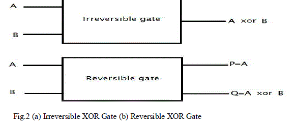
| The block diagram of (irreversible) classical XOR and reversible XOR gate is as shown in figure 2 (a) and (b). |
| 3.1 DEFINITION |
| The multiple output Boolean function F(x1, x2... xn) of n Boolean variable is called reversible if: |
| The number of inputs is equal to the number of outputs (one-to-one mapping). |
| Any output pattern has a unique pre-image. |
| 3.2 REVERSIBLE LOGIC GATES |
| In VLSI design power dissipation is an important factor. The recent computers every time erase a bit of information and dissipate the energy while performing the logical operation. Such logical operations are called "irreversible (classical) |
| logic". The main advantages of reversible logic is low power dissipation, it reduces the information loss in the bit so due to the less information loss power dissipation can be minimized. Reversible logic gate is a k-input, k-output logic device with one-to-one mapping between inputs and outputs. Figure 2(a) and 2(b) shows the classical gate (irreversible gate) and general k X k reversible logic gate. In reversible XOR gate there is no loss of information bit signals. Since one-toone mapping between input vector with output vector gives the equal number of inputs and outputs. |
 |
| The simplest reversible logic gate is Not gate and is also called as 1x1 gate. Controlled Not (CNOT) gate is an example for a 2X2 reversible logic gate. Each reversible logic gate has a cost associated with it and is depends on number of primitive gates used in it called quantum cost. The quantum cost of 1X1 reversible logic gates is zero, and quantum cost of 2X2 reversible logic gates is one. Any reversible logic gate is realized by using 1X1 Not gates and 2X2 reversible gates, such as V and V+ (V is square root and V+ is hermitian of Not gate) and Feynman gate which is also called as controlled Not gate (CNOT). |
| The V and V+ quantum gates have the following property: |
| V X V = NOT |
| V X V+ = V+ X V = I |
| V+ X V+ = NOT |
| The quantum cost of a reversible logic gate can be calculated by counting the number V, V+ and CNOT gates used in implementing it except in few cases. |
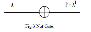
| 3.3 NOT GATE |
| This is the only reversible gate among the conventional logic gates and is also called 1X1 gate. The output of Not gate is simple complimented form of its input. The quantum cost of Not gate is zero. |
 |
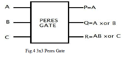
| 3.4 PERES GATE |
| Figure 4 shows a 3X3 Peres gate. The input vector is I (A, B, C) and the output vector is O (P, Q, R). The output is defined by P = A, Q = A xor B and R=AB xor C. Quantum cost of Peres gate is 4. In many designs Peres gate is used because of its lowest quantum cost. Half adder can designed using single Peres gate. |
 |
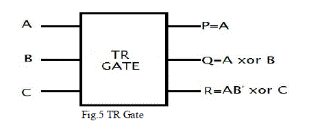
| 3.5 TR GATE |
| TR gate has 3 inputs and 3 outputs having inputs (A, B, C) mapped to outputs (P=A, Q=A xor B, R=AB’ xor C). The quantum cost of TR gate is 4. TR gate can be used in several designs because of its simplicity as well as lowest quantum cost. |
 |
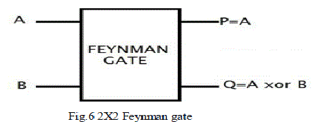
| 3.6 FEYNMAN GATE |
| Feynman gate is a 2X2 reversible gate as shown in figure 6. The input vector is I (A, B) and the output vector is O (P, Q). The outputs are defined as P=A, Q=A xor B. Quantum cost of a Feynman gate is 1.because of its lowest quantum cost it can also be used in several circuit designs. |
 |
IV.PROPOSED METHODOLOGY |
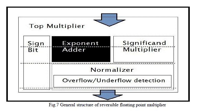 |
| The figure 7 represents the design of reversible single precision floating point multiplier (RSPFPM). Dark portion in the above figure 7 that is reversible exponent adder part is designed and implemented using Verilog code. The coding is done on Xilinx ISE 12.2 for simulation purpose the Modelsim6.3 has been used. So the detailed explanation about the design and implementation of REA is given in following sections. |
| 4.1 SIGN BIT CALCULATION |
| The sign of multiplied product is obtained by the XOR function of X and Y. The XOR function may achieve by a single Peres gate to calculate the sign of the product and will be negative precisely when the signs of the two floating point factors differ from each other. |
| 4.2 EXPONENT ADDER |
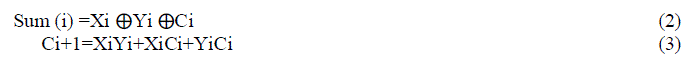
| The exponents are added by using the reversible ripple carry adder and the bias value -127 is subtracted from exponents by using ripple borrow subtractor. The full adder is the basic building block in the ripple carry adder, and most other adder circuits. So in this proposed paper full adder is designed using 2 half adders and a half adder is designed using single Peres gate. Peres gate is used to design half adder because a single Peres gate has an ability to perform all necessary operations required for the half adder circuit and also it has lowest quantum cost. The full adder computes the sum bit Si and carry output bit Ci+1 based on its addend input bits Xi and Yi, and its carry input bit Ci. The sum bit and carry output bits are given in equation below. |
 |
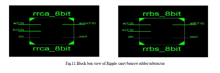
| Reversible ripple carry adder An 8-bit reversible ripple carry adder is used to add the two input exponents. As shown in Figure 8, a ripple carry adder is a chain of cascaded full adders and one half adder. Each full adders has three inputs (A, B, Ci) and two outputs (S, Co). The carry out (Co) of each adder is fed to the next full adder. |
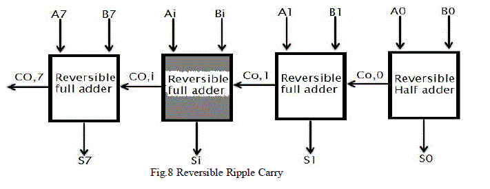 |
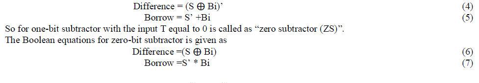
| The addition process produces an 8 bit sum (S7 to S0) and a carry bit (Co, 7). Bias is subtracted from9 bit addition result (S8 to S0). The Bias is subtracted using an array of ripple borrow subtractors. Generally subtractor has three inputs (minuend (S), subtrahend (T), Borrow in (Bi)) and two outputs (Difference (R), Borrow out (Bo)). The subtractor logic can be optimized if one of its inputs is a constant value, in this paper the Bias is constant (127)10 = (001111111)2. |
| The block diagram for one-bit subtractor is shown in Figure 9 for a 1-bit subtractor with the input T equal to 1 is called as “one subtractor (OS)”. |
| The Boolean equations for one-bit subtractor is given as |
 |
 |
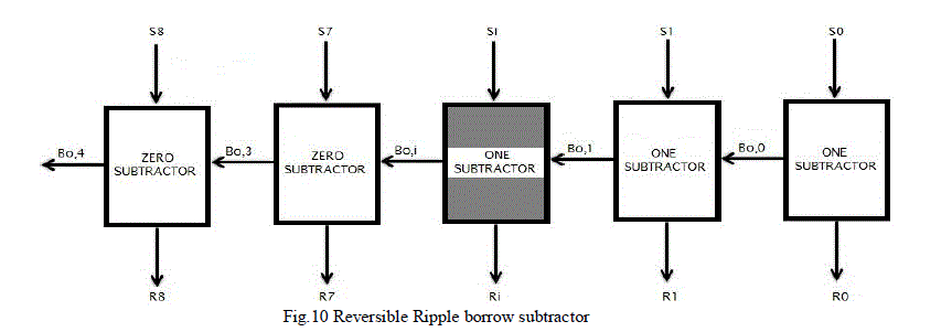
| Figure 10 shows the Bias subtractor which is a chain of 7 one subtractors (OS) followed by 2 zero subtractors (ZS).The borrow output of each subtractor is fed to the next subtractor. |
 |
| The proposed REA in this paper can be used to design the single precision floating point multiplier using reversible logic in order to increase the performance as much as possible. |
V. SIMULATION AND RESULTS |
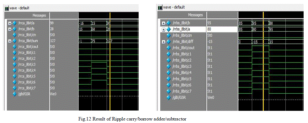
| The entire design of reversible exponent addition using reversible ripple carry adder and reversible ripple borrow subtractor is modelled using Verilog hardware description language .The coding is done on Xilinx ISE 12.2 For simulation purpose the Modelsim6.3 has been used. The simulation result for proposed multiplier is shown in Figure 12. The proposed multiplier uses such exponent part to accomplish its reversible multiplication operation and is efficient in terms of number of reversible gates and garbage output. Reduction in number of gates reduces the complexity of circuit |
 |
 |
VI. APPLICATIONS |
| Reversible computing may have applications in computer security and transaction processing, but the main long-term benefit will be felt very well in those areas which require high energy efficiency, speed and performance. It include the areas like |
| Low power CMOS. |
| Quantum computer |
| Nanotechnology. |
| Optical computing. |
| Designing of low power arithmetic and data path for digital signal processing (DSP). |
VII. CONCLUSION |
| The proposed work presents an implementation of a REA for single precision floating point multiplier using reversible logic that supports the IEEE 754 binary interchange format. Basic reversible gate presented in this paper can be used in regular circuits realizing Boolean functions. The reversible exponent addition using reversible ripple carry adder and reversible ripple borrow subtractor is designed and is modelled using Verilog hardware description language. The proposed multiplier uses such exponent part to accomplish its reversible multiplication operation. Reduction in number of gates to reduce complexity of circuit can be achieved by using reversible logic gates. Reversible computing may have long-term benefit very well in those areas which require high energy efficiency, speed and performance. The future part of the proposed paper may utilizes the reversible multiplier, reversible full adder and half adder for designing optimized multiplier to reduces quantum cost, gate delay and garbage outputs and can improves the performance as much as possible. |
References |
|