International Journal of Advanced Research in Electrical, Electronics and Instrumentation Engineering
ISSN ONLINE(2278-8875) PRINT (2320-3765)
ISSN ONLINE(2278-8875) PRINT (2320-3765)
B.Mehala, Mrs.Anitha Sampath Kumar
|
| Related article at Pubmed, Scholar Google |
Visit for more related articles at International Journal of Advanced Research in Electrical, Electronics and Instrumentation Engineering
This paper describes a resonant circuit based on half-bridge rectifier with auxiliary resonant circuit. Soft switching techniques such as zero current switching (ZCS) and zero voltage switching (ZVS) can be performed by using the auxiliary resonant circuit. The zero current switching can greatly reduce the switching losses and electromagnetic noises. Conduction losses and current stress on switches are reduced greatly. Because circulating current for the soft switching flows only through the auxiliary circuit. Balance output voltage can be obtained using the auxiliary resonant circuit. In this paper the principle of the zero current switching operation, design of the resonant circuits and the control sequence are described from theoretical and practical point of view.
Keywords |
| auxiliary resonant circuit, pulse width modulation technique, balance control technique,(ZCS)zero current switching,(ZVS)zero voltage switching |
1. INTRODUCTION |
| In industrial applications such as ac/dc converters, one of the favorite topology is the half-bridge rectifier. For high efficiency and low electromagnetic interference (EMI) applications, Soft-switching techniques have been developed to reduce switching losses and electromagnetic interference (EMI). Under soft-switching conditions, the switching frequency can be increased to enhance the converter power density. This condition is commonly attained by zero voltage switching (ZVS) and zero current switching (ZCS). An insulated gate bipolar transistor (IGBT) is an appropriate switch for power applications. The ZCS technique is more compatible with the IGBT characteristics since it makes the tailing-current irrelevant [4]. In order to decrease current stresses and conduction losses, unnecessary energy circulation should be prevented and hence unidirectional switches such as the reverse-blocking |
| In general, the soft-switching methods include zero-current-switching (ZCS) and zero voltage-switching (ZVS) depending on the characteristics of the used switches. One of the advantages of using ZCS techniques is the current tail phenomenon in insulated gate bipolar transistor can be eliminated while transited to be off, resulting in less power loss at the transition. Which benefits comprise lower current stress and ZCS on both switches compared to traditional resonant circuits applied to power converters has two resonant frequencies in operation and is more complicated than the other circuit which has only one resonant frequency. |
| Based on the advantages of soft-switching, this paper provides a novel ZCS-pulse width modulation (PWM) halfbridge boost to increase the efficiency and restrain EMI. Although the half-bridge rectifier can provide double dc output voltages on the two split capacitors, it is an important issue that the two dc output may cause imbalance problem, but they are only suitable for the specific PWM controllers and associated control strategies, that is, modifications and variations must be made for the used controller. |
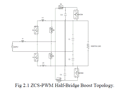
II. CIRCUIT DIAGRAM FOR PROPOSED SYSTEM |
 |
| Before analysis, some assumptions are made: |
| a) All elements are considered as ideal, with no parasitic components. |
| b) Voltages across the output capacitors are equal, Vo1 = Vo2 = E and Vo1 + Vo2 = 2E = Vo due to balance control. |
| c) Input current is considered as a constant within one switching period, is = Is; and |
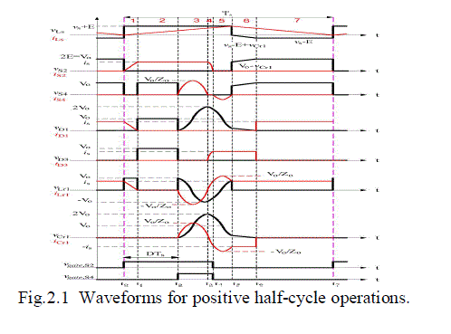
| d) Resonant capacitor voltages are zero, vCr= 0, and resonant inductor currents are equal to input current, iLr= Is, when t ≤ t0. During t ≤ t0, the primary switch S2 keeps the off state and the input current Is flow through the diode D1, the resonant inductor Lr1, and the output capacitor C1 so that C1 is charged and Lr1 is demagnetized. The operation analysis for positive half-cycle consists of seven periods. |
 |
III. MODES OF OPERATION |
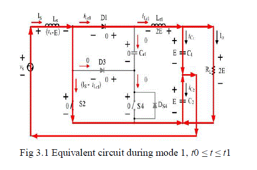
| Mode 1, [t0 ≤ t ≤ t1]: In this duration primary active switch S2 is turned on, and the input current is passes through S2, while t = t0. The resonant inductor current goes to zero, iLr1 = 0, so that the free-wheeling diode D1 is turned off with ZCS, while t = t |
| iLr1 =Is –Vo/ Lr1 (t − t1) |
| vCr1 =0 |
| and the time interval during the first period, t1 − t0, |
| can be computed as |
| Δt1 = IsLr1/Vo |
 |
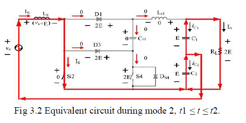
| Mode 2, [t1 ≤ t ≤ t2]: The primary switch S2 is still on, and other elements all are off while t = t1. During this time interval, the input inductor Ls is magnetized by the input voltage vs and the voltage across C2, the input current Is passes through S2 and discharges C2, the equivalent circuit Based on the analysis as above, the equations related to the voltage across Ls and the resonant tank can be derived as |
| vLs(t) =vs+ E |
| iLr1(t) =0 |
| vCr1(t) =0 |
| The time interval during the second period, t2 − t1, can be computed as |
| Δt2 = DTs − Δt1 |
| Where D is duty cycle and Ts is switching period. |
 |
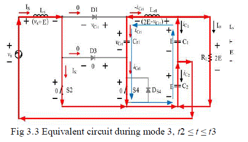
| Mode 3, [t2 ≤ t ≤ t3]: The auxiliary switch S2 is turned on while t = t2, two output voltages across capacitors C1 and C2 and the resonant elements Lr1 and Cr1 form the resonant path, the input inductor Ls is kept to be magnetized, the input current Is passes through S2 and discharges C2 with the resonant current iLr1, the equivalent circuit Based on the analysis as above, the equations related to the resonant tank can be derived as |
| iLr1(t) = −Vo/Zosin ωr(t − t2) |
| vCr1(t) = Vo − Vo cosωr(t − t2) |
| Zo=√Lr1/Cr1 |
| ωr=1 √Lr1Cr1 |
| Wherein Zo is the characteristic impedance and ωr is the resonant radius frequency, |
| ωr= 2πfr |
| The time interval during the third period, t3 − t2, can be Computed as |
| Δt3 = π/ω r |
| This duration ends at t = t3, and the voltage across the |
| Resonant capacitor Cr1 is |
| vCr1, peak= vCr1(t3) = 2Vo. |
 |
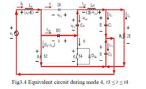
| Mode 4, [t3 ≤ t ≤ t4]: The resonant capacitor Cr1 is discharged to provide energy for the resonant tank while t =t3. The current iCr1 passes through the output capacitor C1 and C2, the resonant tank elements Lr1 and Cr1, the primary switch S2, and the diode D3 so that the auxiliary at this time and the current passes through S2 is that iS2 = Is − iLr1. Also, the primary switch S2 is turned off with ZCS while iLr1 =Is. The equivalent circuit is shown in Fig. 9, and based on the analysis as above, the equations related to the voltage across Ls and the resonant tank can be derived as |
| iLr1(t) = Vo /Zosin ωr(t − t3) |
| vCr1(t) = Vo + Vo cosωr(t − t3) |
| and the time interval during fourth period, t4 − t3, can be computed as |
| Δt4 =1/ωrsin−1(IsZo/Vo). |
 |
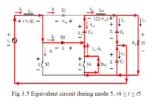
| Mode 5, [t4 ≤ t ≤ t5]: Because the resonant current will be larger than the input current iLr1 ≥ Is while t = t4, the current passing through DS4 is iLr1 − Is. The equivalent circuit is shown, and the related equations are the same as those during fourth period |
| iLr1(t) = Vo/Zosin ωr(t − t4) |
| vCr1(t) = Vo + Vo cosωr(t − t4) |
| and the time interval during fifth period, t5 − t4, can be computed as |
| Δt5= π/ωr− 2Δt4 |
 |
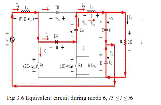
| Mode 6, [t5 ≤ t ≤ t6]: The resonant capacitor Cr1 is discharged by the input current Is and the input inductor Ls is demagnetized while iLr1 = Is. Based on the analysis as above, the equations related to the voltage across Ls and the resonant tank can be derived as |
| vLs= vs− E + vCr1 |
| vCr1 = vCr1(t5) – Is/Cr1(t − t5) |
| vLr1(t) = 0 |
| iCr1(t) = −Is |
| and the time interval during sixth period, t6 − t5, can be computed as |
| Δt6 = 2VoCr1/Iscos [ωr(Δt4 +Δt5)] |
 |
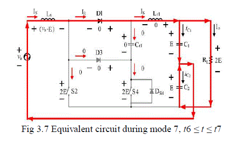
| Mode 7, [t6 ≤ t ≤ t7]: The free-wheeling diode D1 is turned on with ZVS because vcr1 (t6) = vD1(t6) = 0 while t = t6. The input inductor Ls continues to be demagnetized and the equivalent circuit. Based on the analysis as above, the equations related to the voltage across Ls and the resonant tank can be derived as |
| vLs=vs− E |
| iLr1 =Is |
| vCr1 =0 |
| and the time interval during seventh period, t7 − can be computed as |
| Δt7 = Ts− DTs − 2π/ω r+Δt4 − Δt6 |
 |
| In order to achieve ZCS on the primary switch and the auxiliary switch based on the analysis as above, the condition can be derived as |
| Vo/Zo≥ Is,peak |
| Where Is, peak is the peak value of the input current. |
IV.HALF BRIDGE RESONANT AC-DC CONVERTER |
| Fig 4.1 shows the half bridge ac-dc converter with auxiliary resonant circuit. The proposed circuit consist of AC input source, half bridge boost rectifier, auxiliary resonant circuit ,filter capacitors and load. The half bridge made up of IGBT switches with capacitors is used to perform the AC to DC conversion with boost operation also. |
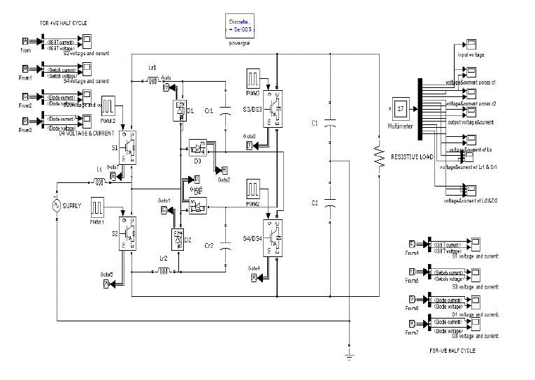 |
| The auxiliary resonant circuit consist of auxiliary switches ,resonant inductor and resonant capacitors is used to perform zero current switching(ZCS) .the suitable PWM techniques are designed to perform the operation with high efficiency. |
V. SIMULATION RESULTS |
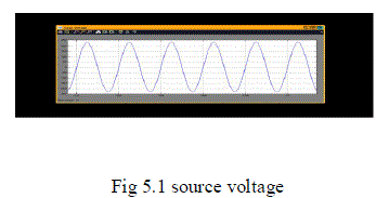
| The half bridge ac-dc converter with auxiliary resonant circuit is simulated by using matlab/Simulink. The driving pulses, voltage across MOSFET switches, voltage across load and voltage across capacitors are shown in below. Fig 5.1 shows voltage across the input AC source .from this waveform we conclude that we can also perform the power factor correction on input side. |
 |
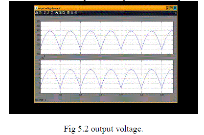
| The voltage across the load resistor are shown in fig 5.2. |
| Form this figure we can conclude that the rectified output DC output is boosted upto 400 volts. |
 |
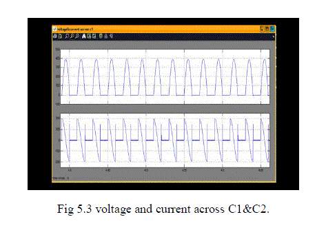
| The voltage across capacitor 1 and capacitor 2 are shown in fig 5.3. from this result the voltage across the capacitor 1 and voltage across capacitor 2 both are equal in magnitude.from this we can conclude that we can perform the volatge balanced control also by using auxilary resonsnt circuit. |
 |
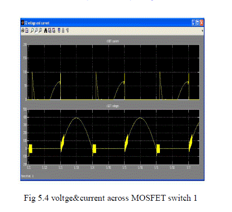
| Zero current switching operation is performed by means of auxiliary resonant circuit. The voltage and current across switch 1 are shown in fig 5.4. |
 |
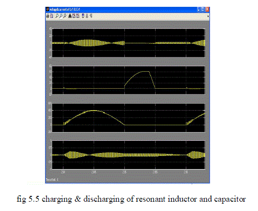
| The charging and discharging of auxiliary resonant inductor and capacitor are shown in fig 5.5. |
 |
VI.CONCLUSION |
| This paper proposes and implements a novel ZCS-PWM half-bridge boost with two output voltage balance control. Steady-state analyses including seven modes for positive half cycle was performed in detail. The small-signal analysis was discussed, and design of the corresponding current and voltage error amplifiers was realized. The balance control scheme for two output capacitor voltage was designed and implemented to eliminate the inherent imbalance phenomenon. Compared to conventional half-ridge rectifier, benefits of the proposed novel ZCS-PWM half-bridge boost include: 1) soft-switching comprising ZCS and ZVS without extra stress; 2) high efficiency because of ZCS in active switches and ZVS in passive switches; 3) two output voltage balance without influencing power factor; and 4) easy and simple design and implementation because of using off-self PWM IC. Design and implementation of an exemplary novel ZCS-PWM half-bridge boost with output voltage balance control have verified the system performance. |
ACKNOWLEDGEMENT |
| With profound sense and regards, I acknowledge with great pleasure the guidance and support extended by Mrs.V.Jayalakshmi, Assistant Professor and Head, Department of Electrical and Electronics and Engineering, for the support, encouragement and the facilities provided to me during this project. I express heartfelt thanks to my project guide Mrs.Anithasampathkumar, Assistance professor, Department of Electrical and Electronics and Engineering, for her continual guidance & support with her suggestion for the successful completion of the project |
References |
|