International Journal of Advanced Research in Electrical, Electronics and Instrumentation Engineering
ISSN ONLINE(2278-8875) PRINT (2320-3765)
ISSN ONLINE(2278-8875) PRINT (2320-3765)
C Anusuya1, Mr. S.Venkatasubramanian2
|
| Related article at Pubmed, Scholar Google |
Visit for more related articles at International Journal of Advanced Research in Electrical, Electronics and Instrumentation Engineering
this paper proposes a high step-up solar power optimizer (SPO) that efficiently harvests maximum energy from a photovoltaic (PV) panel then outputs energy to a dc-micro-grid. The existing structure integrates coupled inductor and switched capacitor technologies to realize high step-up voltage gain. The proposed system enhances the features of Dual Active Bridge and perturbation and observation algorithm for tracking the maximum power and to step up the input power. The photovoltaic energy is harvested and given to Dual Active Bridge circuit where it can be highly stepped up using linear tansformer.The linear transformer turns ratio is 1:4 and this output is again given to the converter bridge .The converter changes AC into DC.This dc power is given as a input to the dc distribution system. This method has high efficiency and easy implementation. Number of components used for its implementation also lesser than existing systems. The dual active bridge is simulated using MATLAB/ SIMULINK software for different solar panel power. Index Terms—Dual Active Bridge, Maximum Power Point Tracking algorithm, photovoltaic panel
Keywords |
| Dual Active Bridge, Maximum Power Point Tracking algorithm, photovoltaic panel |
I. INTRODUCTION |
| Fossil fuels continue to be depleted, and their use has been instrumental to climate change, is a problem that grows more severe each year. A photovoltaic (pv) power generation system, which uses a renewable resource, has been extensively used in emergency facilities and in generating electricity for mass use a conventional PV generation system is either a single or a multi string PV array that is connected to one or several central PV Numerous series connected PV modules are connected in the PV array to achieve the DC link voltage that is enough to be connected to electricity connected to electricity through the DC AC inverter. However, the power reduction that is caused by the shadow effect is an inevitable problem in a centralized PV system. The use of a micro-inverter or ac module has recently been proposed for individual PV panels. Although this discrete PV power generation solution may partially eliminate the shadow problem, a microinverter structure constrains the system energy’s harvesting efficiency and entails high costs. |
| A solar power optimizer (SPO) was developed as an alternative to maximize energy harvest from each individual PV module. An SPO is used as a dc-dc converter with Maximum Power Point Tracking (MPPT), which increases PV panel voltage to optimum voltage levels for a dc micro-grid connection or through a dc-dc inverter for electricity.Fig.1.1shows a single PV panel’s energy. PV solar electricity together with solar thermal has the highest potential of all the renewable energies since solar energy is a practically unlimited resource, available everywhere. |
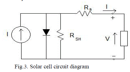
| The power delivered by the PV module depends on their radiance, temperature, and shadowing conditions. The PV panel has a nonlinear characteristic, and the power has a Maximum Power Point (MPP) at a certain working point, with coordinates VMPP voltage and IMPP current. Since the MPP depends on solar irradiation and cell temperature, it is never constant over time; thereby Maximum Power Point Tracking (MPPT) should be used to track its changes. |
II. BLOCK DIAGRAM OF SOLAR POWER OPTIMIZER |
| The proposed system is having dual active bridge as the type of dc-dc boost converter and it replaces the coupled inductor by using this component. The microcontroller has been embedded with the perturb and observe algorithm as which is the simple method and tracks maximum power easily and balancing the dc link voltages. |
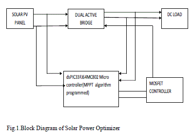 |
| The solar panel is connected to dual active bridge and its voltage and current are sensed by maximum power point controller. It tracks the maximum power point and obtain maximum power from the panel using perturb and observe method. This maximum power is given to dual active bridge and it is given to dc load .The dual active bridge contains two voltage sourced full bridge circuits or half bridge circuits (or even push-pull circuits) and a HF transformer. The reactive network simply consists of an inductor L connected in series to the HF transformer; hence, the DAB directly utilizes the transformer stray inductance. Due to the symmetric circuit structure, the DAB readily allows for bidirectional power transfer. The main advantage of the DAB is the low number of passive components, the evenly shared currents in the switches, and its soft switching properties. With the DAB converter topology, high power density is feasible. |
III. DUAL ACTIVE BRIDGE |
| A dual active bridge (DAB) converter with high power density and soft switching operation is proposed as a bidirectional DC to DC interface to convert electric energy between a low voltage battery and a high voltage DC bus . It is a DC-AC-DC converter which allows energy transfer between the source and the load. It is a buck and a boost bidirectional converter isolated by a high frequency transformer. |
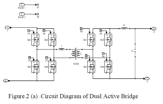 |
| The source side and the load side both are full- bridge circuits, operated at a fixed frequency. The two full bridges are connected via a high frequency transformer. Full bridge circuits have minimal voltage and current stresses in the devices and minimum VA rating of the transformer. High frequency transformer can integrate different voltage levels with the turn ratio of the transformer. It also provides electrical isolation, which may be required by the industry standard. Finally, the leakage inductor of the transformer can be used as an energy transfer element. In every cycle, a small fraction of energy from the source is stored in this leakage inductor before it is transferred to the load. The inductance can be added by using external inductors connected in series with the transformer. Below Figure shows the circuit for DAB converter. The switches of the DAB circuit are operated at a constant frequency. The switches are operated at a fixed frequency and with a fixed duty cycle of 50%. |
IV. MODULATION STRATEGIES FOR DAB DC-DC CONVERTER |
| Three types of modulation strategies have been analyzed for DAB DC-DC converter |
| Phase shift modulation |
| Triangular modulation |
| Trapezoidal modulation |
| Phase Shift (PS) modulation |
| Phase shift modulation is the widely used technique in dual active bridge converter. For phase shift operation, rectangular transformer voltages vT1 (t) and vT2(t) with switching frequency fS and phase shift, are applied to the transformer and the converter inductance L. The power transfer is controlled by the phase shift angle ÃÂÃâ¢. The higher the phase difference, the higher is the power transferred. It is given by the equation, |
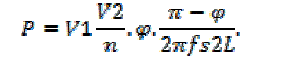 |
| Phase shift modulation is very simple to implement. It is possible to use half bridge circuits to generate the high frequency transformer voltages vT1 (t) and vT2 (t). Less number of power electronic devices. The disadvantage is a high level of reactive power circulates in the high frequency transformer when the operating point is significantly different to the nominal operating point. For phase shift modulation it is not possible to directly influence the shape of the transformer current since it depends on the DC voltages V1 and V2 as well as on the phase shift ÃÂÃâ¢. TRIANGULAR MODULATION |
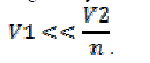
| Triangular modulation is used when the voltages V1 and V2 are significantly different. This modulation method can be implemented when the transformer has a turns ratio given by |
 |
| The switching pattern for triangular modulation is shown below |
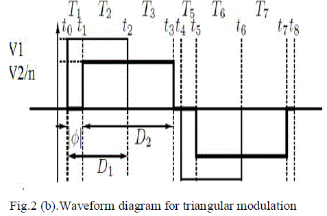 |
| The advantages and disadvantage of triangular modulation are, this method allows for the implementation of ZCS for the low voltage side, which is desired for low switching losses, high switching speed, and low EMI. In this method the parasitic inductors of the low voltage side switches are utilized as part of the converter inductance L. It is particularly interesting for the specific converter because of the low value of inductance L. Ineffective converter utilization. |
V. TRAPEZOIDAL MODULATION |
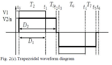
| The trapezoidal modulation method can be implemented when the transformer has a turn’s ratio given by V1 ≈ V2/n. The advantages of trapezoidal modulation are Good converter efficiency is achieved. This is because the full bridge circuits are operating with large duty cycles. Results in a lower RMS current than for triangular modulation. Switching losses are less compared to phase shift modulation. The switching pattern for trapezoidal modulation is shown below. |
 |
| SOLAR PANEL: |
| A solar panel (photovoltaic module or photovoltaic panel) is a packaged, interconnected assembly of solar cells, also known as photovoltaic cells. The solar panel can be used as a component of a larger photovoltaic system to generate and supply electricity in commercial and residential applications. Because a single solar panel can produce only a limited amount of power, many installations contain several panels. A photovoltaic system typically includes an array of solar panels, an inverter, and sometimes a battery and interconnection wiring. |
| THEORY AND CONSTRUCTION: |
| Solar panels use light energy (photons) from the sun to generate electricity through the photovoltaic effect. The structural (load carrying) member of a module can either be the top layer or the back layer. The majority of modules use wafer-based crystalline silicon cells or thin-film cells based on cadmium telluride or silicon. The conducting wires that take the current off the panels may contain silver, copper or other conductive (but generally not magnetic) transition metals. The cells must be connected electrically to one another and to the rest of the system. Cells must also be protected from mechanical damage and moisture. Most solar panels are rigid, but semi-flexible ones are available, based on thin-film cells. Electrical connections are made in series to achieve a desired output voltage and/or in parallel to provide a desired current capability. Separate diodes may be needed to avoid reverse currents, in case of partial or total shading, and at night. The p-n junction’s of monocrystalline silicon cells may have adequate reverse current characteristics that these are not necessary. Reverse currents waste power and can also lead to overheating of shaded cells. Solar cells become less efficient at higher temperatures and installers try to provide good ventilation behind solar panels. Some recent solar panel designs include concentrators in which light is focused by lenses or mirrors onto an array of smaller cells. This enables the use of cells with a high cost per unit area in a cost-effective way. |
 |
| Depending on construction, photovoltaic panels can produce electricity from a range of frequencies of light, but usually cannot cover the entire solar range (specifically, ultraviolet, infrared and low or diffused light). Hence much of the incident sunlight energy is wasted by solar panels, and they can give far higher efficiencies if illuminated with monochromatic light. |
| Therefore another design concept is to split the light into different wavelength ranges and direct the beams onto different cells tuned to those ranges. This has been projected to be capable of raising efficiency by 50%. The use of infrared photovoltaic cells has also been proposed to increase efficiencies, and perhaps produce power at night. Currently the best achieved sunlight conversion rate (solar panel efficiency) is around 21% in commercial product, typically lower than the efficiencies of their cells in isolation. The Energy Density of a solar panel is the efficiency described in terms of peak power output per unit of surface area, commonly expressed in units of Watts per square foot (W/ft2). |
| STANDALONE PV SYSTEM COMPONENTS PV CELL |
| A photovoltaic cell or photoelectric cell is a semiconductor device that converts light to electrical energy by photovoltaic effect. If the energy of photon of light is greater than the band gap then the electron is emitted and the flow of electrons creates current. However a photovoltaic cell is different from a photodiode. In a photodiode light falls on n channel of the semiconductor junction and gets converted into current or voltage signal but a photovoltaic cell is always forward biased. |
| PV MODULE |
| Usually a number of PV modules are arranged in series and parallel to meet the energy requirements. PV modules of different sizes are commercially available (generally sized from60W to 170W). For example, a typical small scale desalination plant requires a few thousand watts of power. |
| MOSFET DRIVE IRS2110 |
| The IR2110/IR2113 are high voltage, high speed power MOSFET and IGBT drivers with independent high and low side referenced output channels. Logic inputs are compatible with standard CMOS or LSTTL output, down to 3.3V logic. |
| The output drivers feature a high pulse current buffer stage designed for minimum driver cross-conduction. Propagation delays are matched to simplify use in high frequency applications. The floating channel can be used to drive an N-channel power MOSFET or IGBT in the high side configuration which operates up to 500 or 600 volts. |
| DsPIC33FJ32MC302/304,dsPIC33FJ64MCX02/X04 &dsPIC33FJ128MCX02/X04 SYSTEM MANAGEMENT: |
| Flexible clock options: - External, crystal, resonator, internal RC - Fully integrated Phase-Locked Loop (PLL) - Extremely low jitter PLL , Power-up Timer, Oscillator Start-up Timer/Stabilizer ,Watchdog Timer with its own RC oscillator Fail-Safe Clock Monitor (FSCM), Reset by multiple sources. |
| POWER MANAGEMENT: |
| On-chip 2.5V voltage regulator, Switch between clock sources in real time, Idle, Sleep, and Doze modes with fast wake-up |
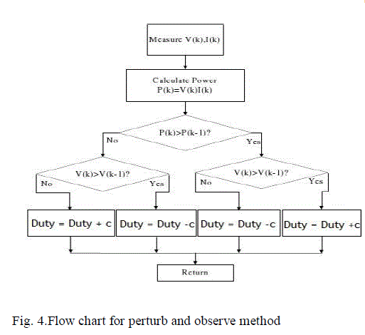
| IMPLEMENTATION OF MPPT USING MATLAB PERTURB AND OBSERVE ALGORITHM (P&O) |
| The Perturb & Observe algorithm states that when the operating voltage of the PV panel is perturbed by a small increment, if the resulting change in power P is positive, then we are going in the direction of MPP and we keep on perturbing in the same direction. If P is negative, we are going away from the direction of MPP and the sign of perturbation supplied has to be changed. |
 |
VI. SIMULATION |
| MATLAB is a high-performance language for technical Computing. It integrates computation, visualization, and programming in an easy-to-use environment where problems and solutions are expressed in familiar mathematical notation. |
| SIMULATION RESULTS FIXED RADIATION |
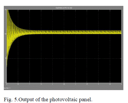 |
| photovoltaic array. These current and voltage waveforms are obtained using Simulink/Matlab. This array is having five panel which has been arranged serious and parallel. Each panel is connected both seriously and parallel. The output voltage 100v is given to the dual active bridge. |
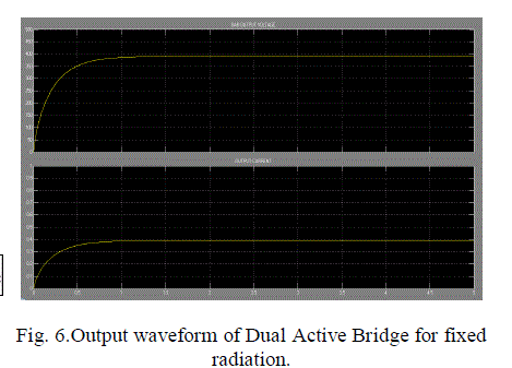 |
| The Fig.6 shows the output voltage of dual active bridge. The output voltage is stepped up to 400v.The dual active bridge is having linear transformer in between the two group of bridges. So that the 100v is stepped up into 400v and which is given to the converter. This converter converts ac into dc and then sends to dc load as their input. |
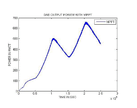
| VARIABLE RADIATION |
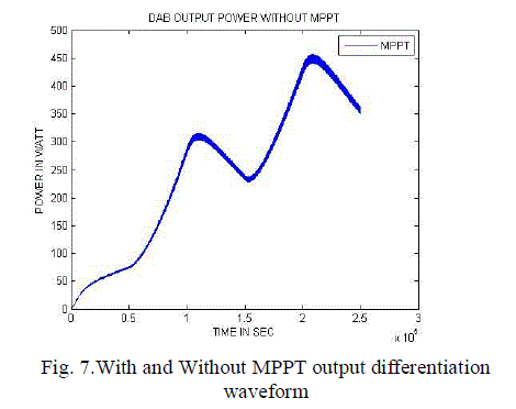
| The solar panel is set to track variable radiation using maximum power point tracking algorithm. For different solar radiation the output of dual active bridge is shown below. The output of the dual active bridge is reached up to 620w when MPPT is enabled. The output is 450w when MPPT is not enabled. |
 |
 |
VII. CONCLUSION |
| This paper has provided a brief summary of solar power optimizer using MATLAB simulation. In this project, initially, the variation is fixed as 20000w/m2and then simulated. For different radiation the output has been simulated using MATLAB. The result of this paper is using MPPT algorithm the maximum output is obtained and then stepped up. It is clearly showed and differentiated in the last section of Fig.7.Thus solar power optimizer for dc distributed system is implemented using MPPT algorithm and Dual Active Bridge circuit and verified that obtained output is efficient. |
References |
|