International Journal of Advanced Research in Electrical, Electronics and Instrumentation Engineering
ISSN ONLINE(2278-8875) PRINT (2320-3765)
ISSN ONLINE(2278-8875) PRINT (2320-3765)
Khumanthem Devjit Singh, K. Jyothi
|
| Related article at Pubmed, Scholar Google |
Visit for more related articles at International Journal of Advanced Research in Electrical, Electronics and Instrumentation Engineering
Multiplication is most commonly used operation in mathematics. Integer multiplication is used commonly in the real world, and binary multiplication is the basic multiplication used for the integer multiplication. Systolic algorithms are the efficient algorithms to perform the binary multiplication. Systolic array is an arrangement of processors in an array where data flows synchronously across the array between neighbors, usually with different data flowing in different directions. Each processor at each step takes in data from one or more neighbors (e.g. North and West), processes it and, in the next step, outputs results in the opposite direction (South and East). The present work is concentrated on developing hardware model for systolic multiplier using Verilog HDL (Hardware Description Language) as a platform. The design is simulated using modelsim simulator and synthesized on Spartan 3 FPGA Board.
Keywords |
| Systolic Array, Parallel Processing, Xilinx, FPGA, VHDL. |
I. INTRODUCTION |
| The paper briefs about the method to verify appropriate program execution. In order to achieve the high speed and low power demand in DSP applications, parallel array multipliers are widely used. In DSP applications, most of the power is consumed by the multipliers. Hence, low power multipliers must be designed in order to reduce the power dissipation in DSP applications. Systolic algorithm is the form of pipelining, sometimes in more than one dimension. In this algorithm data flows from a memory in a rhythmic fashion, passing through many processing elements before it returns to memory. H. T. Kung and Charles Leiserson were the first to publish a paper on systolic arrays in 1978, and coined the name, which refers to the “pumping action of the heart’’. What can a systolic array do? This question is very important, and the answer is that every Sequential algorithm that can be transformed to a parallel version suitable for running on array processors that execute operations in the so-called systolic manner, and systolic array is one of solutions to the need for a highly parallel computational power. Due to the use of matrix-multiplication algorithm in wide fields such as Digital Signal Processing (DSP), image processing, solutions of differential comparison, nonnumeric application, and complex arithmetic operations, we shall design an 8-bit systolic array that designed and implements. Verilog finds many applications because of its very high speed integrated circuit. It is a hardware description language and program can be loaded into the chip and can be used by tool user. As the language supports flexible design methodology, it can be used to define complex electronic systems. Common language can be used to describe the library components. Because of its unique feature, Verilog is used to design N-bit binary multiplier. The program in Verilog provides the scope for multiplication of two N-bit binary numbers by including the user defined package. |
II. PURPOSE OF IMPLEMENTATION |
| The purpose of this implementation is to efficiently resolve a wide spectrum of computational problems by designing and implementing the systolic array architecture on FPGA. Designers search for high performance and flexible architectures; so this paper introduces one of the most efficient ways to meeting them. The systolic array combines different properties that are seldom found together. These properties are |
| 1) Flexible hardware and software (i.e. FPGA technology). |
| 2) Spatial and temporal parallelism (i.e. systolic array Architecture). |
| 3) Easily scalable architecture. |
| 4) High degree of pipelining. |
III. DESIGN METHODOLOGY |
| In systolic multiplication, to carry out the multiplication and get the final product following steps should be followed |
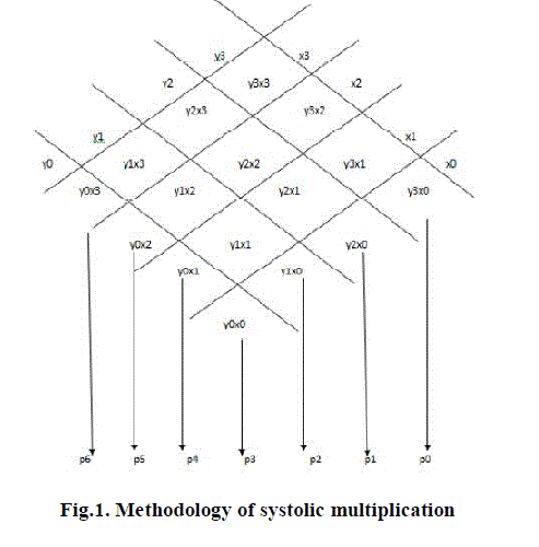
| 1. The multiplicand and multiplier are arranged in the form of array as shown in the Fig.1 |
| 2. Each bit of multiplicand is multiplied with each bit of multiplier to get the partial products. |
| 3. The partial products of the same column are added along with carry generated. |
| 4. So the resulted output by adding partial products and the carry is the final product of the two binary numbers. |
 |
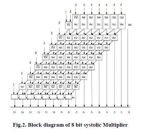 |
| Figure shows the functional units of the 8 bit Systolic Multiplier. Each unit is an independent processing unit. These units share information with their neighbors, after performing the needed operations on the data. Each box in the Fig. represents a full adder. Inputs vector X and Y are ANDed and the AND outputs are fed as input to full adder, which gives rise to two outputs. One is the actual multiplied output vector Z and another one is the carry generated from the addition of the AND output, which is further used by other full adders. In this way computation takes place simultaneously in the rows and columns. All the inputs are applied simultaneously, therefore registers are not required. Availability of inputs at the start of the computation and the systolic array structure helps the multiplier to perform faster compared to other multipliers. |
IV. IMPLEMENTATION |
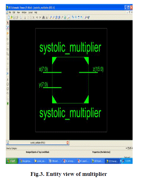
| The programming environment for implementing the circuit is based on Verilog. In our implementation Systolic Array Multiplier is designed for 8 bits using structural and behavioral styles and is implemented, tested on the Spartan-3 FPGA board. Obtained results are accurate and error free. In structural modeling, multiplier is divided into 3 sections i.e. upper, middle and lower sections. Where, all the three sections operate on the data simultaneously. Full adder and AND gates are basic building blocks of the multiplier. Each section has 8 full adders and associated AND gates. The entity part or the peripheral view of the multiplier is given in Fig. 3 |
 |
| The behavioral description is written and implemented based on behavior of the Systolic Array multiplier. A timing analysis tool is then applied to the object module to determine maximum operating speed. If algorithms are time consuming then the efficiency of multiplier decreases because, in recent days the efficiency is measured not only with the accuracy but also with the speed. As FPGA is purely hardware circuit, the time taken by it to execute the algorithm is much less. Thus, the Systolic multiplication algorithm implemented on FPGA works faster than any other multiplication technique. |
V. DEVICE UTILIZATION SUMMARY |
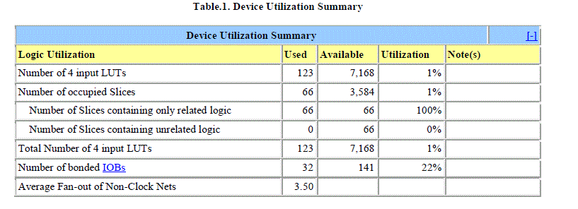 |
| Table shows the device utilization summary obtained from the synthesis report of structural modeling respectively. By analyzing the synthesis results there is drastic reduction of resources of FPGA when modeled with two different styles and power consumption is also reduced to a greater extent. Because of this implementation, system requires very less space while designing hardware and eliminates the complexity in hardware design. |
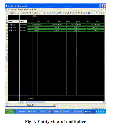 |
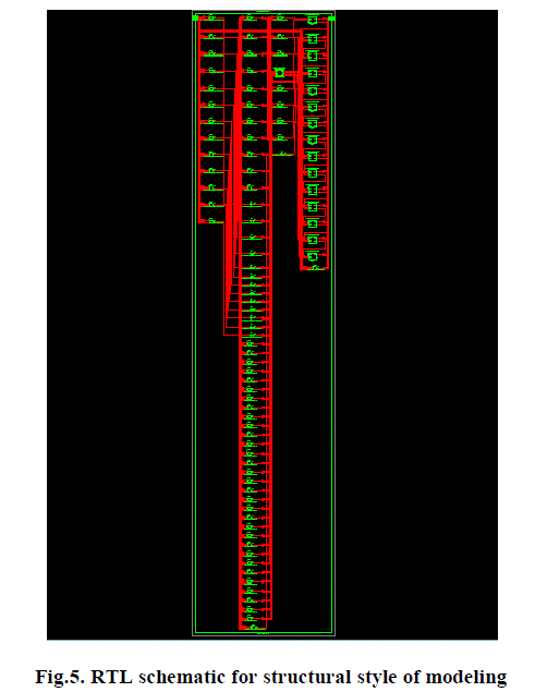
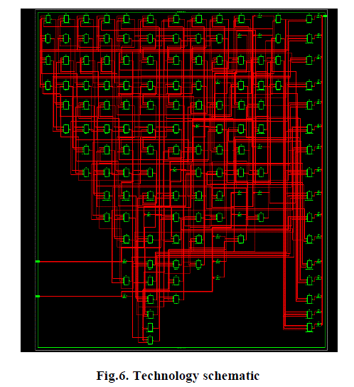
| Simulation results are as shown in the Fig. 4 for inputs 11001100 and 01100110 and the output obtained is 1110101101001000. Fig. 5 and Fig.6 shows the RTL schematic of the 8 bit Systolic Array Multiplier obtained by using structural style of modeling. |
 |
 |
VI. CONCLUSION |
| Thus the design of 8 bit Systolic Array Multiplier design was optimized using structural style compared with behavioral style. The designed circuit has been implemented on FPGA and simulated using Isim simulator version 14.3 simulation software and the results are up to the mark. Again, using Xilinx XST we have synthesized the design on Spartan 3e board effectively. By implementing such designs in Verilog one easily understands the behavior of designing aspects effectively. If this prototype is implemented in real time then there will be number of advantages benefited to the mankind. |
References |
|