International Journal of Advanced Research in Electrical, Electronics and Instrumentation Engineering
ISSN ONLINE(2278-8875) PRINT (2320-3765)
ISSN ONLINE(2278-8875) PRINT (2320-3765)
Velicheti Swetha1, S Rajeswari2
|
| Related article at Pubmed, Scholar Google |
Visit for more related articles at International Journal of Advanced Research in Electrical, Electronics and Instrumentation Engineering
Now-a-days Power consumption (or) power dissipation has becomes the most important criteria for implementing anyone of the digital circuit. While calculating the efficient value of the output of that particular digital circuit, we may use the concept of scaling. But, while increasing the scaling process there may be a loss of leakage current. Due to the leakage current the usage of power (power dissipation) is increased. For removing these kinds of leakage currents we are going to use “power gating techniques”. By using the power gating techniques we can provide better power efficiency also. In this paper we are going to analyze the digital circuits using different types of power gated circuits with the help of low power VLSI design techniques. By using the nanometer technology we may get different results for different digital power gating circuits. The entire procedure may implement and simulated using Micro-wind Layout Editor & D. Sch (Digital Schematic).
Keywords |
| Power gating circuits, Ground bounce noise, sleep methods. |
I. INTRODUCTION |
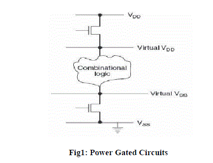
| The scaling of process technologies to nanometer regime has resulted in a rapid increase in leakage power dissipation. Hence, it has become extremely important to develop design techniques to reduce static power dissipation during periods of inactivity. The power reduction must be achieved without trading-off performance which makes it harder to reduce leakage during normal (runtime) operation. On the other hand, there are several techniques for reducing leakage power in sleep or standby mode. Power gating [8] is one such well known technique where a sleep transistor is added between actual ground rail and circuit ground (called virtual ground). This device is turned-off in the sleep mode to cut-off the leakage path. It has been shown that this technique provides a substantial reduction in leakage at a minimal impact on performance. Power gating technique uses high Vt sleep transistors which cut off VDD from a circuit block when the block is not switching. The sleep transistor sizing [6] is an important design parameter. This technique, also known as MTCMOS, (or) Multi-Threshold CMOS reduces stand-by or leakage power, and also enables Id testing. |
| Power gating affects design architecture more than clock gating. It increases time delays as power gated modes have to be safely entered and exited. Architectural trade-offs exist between designing for the amount of leakage power saving in low power modes and the energy dissipation to enter and exit the low power modes. Shutting down the blocks can be accomplished either by software (or) hardware. Driver software can schedule the power down operations. Hardware timers can be utilized. A dedicated power management controller is another option. |
| An externally switched power supply is a very basic form of power gating to achieve long term leakage power reduction. To shut off the block for small intervals of time, internal power gating is more suitable. CMOS switches that provide power to the circuitry are controlled by power gating controllers. Outputs of the power gated block discharge slowly. Hence output voltage levels spend more time in threshold voltage level. This can lead to larger short circuit current. Power gating uses low-leakage PMOS transistors as header switches to shut off power supplies to parts of a design in standby (or) sleep mode. Inserting the sleep transistors splits the chip's power network into a permanent power network connected to the power supply and a virtual power network that drives the cells and can be turned off. |
 |
II. POWER-GATING PARAMETERS |
| Power gating implementation has additional considerations for timing closure implementation. The following parameters need to be considered and their values carefully chosen for a successful implementation of this methodology. |
| 1. Power gate Size: The power gate Size must be selected to handle the amount of switching current at any given time. The gate must be bigger such that there is no measurable voltage (IR) drop due to the gate. As a rule of thumb, the gate Size is selected to be around 3 times the switching capacitance. Designers can also choose between header (P-MOS) or footer (N-MOS) gate. Usually footer gates tend to be smaller in area for the same switching current. Dynamic power analyNMOS1s tools can accurately measure the switching current and also predict the Size for the power gate. |
| 2. Gate control slew rate: In power gating, thiNMOS1s an important parameter that determines the power gating efficiency. When the slew rate is large, it takes more time to switch off and switch-on the circuit and hence can affect the power gating efficiency. Slew rate is controlled through buffering the gate control Signal. |
| 3. Simultaneous switching capacitance: This important constraint refers to the amount of circuit that can be switched simultaneously without affecting the power network integrity. If a large amount of the circuit is switched simultaneously, the resulting "rush current" can compromise the power network integrity. The circuit needs to be switched in stage in order to prevent this. |
| 4. Power gate leakage: Since power gates are made of active transistors, leakage reduction is an important consideration to maximize power savings |
| i) Fine-grain power gating: |
| Adding a sleep transistor to every cell that is to be turned off imposes a large area penalty, and individually gating the power of every cluster of cells creates timing issue introduced by inter-cluster voltage variation that are difficult to resolve. Fine-grain power gating encapsulates the switching transistor as a part of the standard cell logic. Switching transistors are designed by either the library IP vendor or standard cell designer. Usually these cell designs conform to the normal standard cell rules and can easily be handled by EDA tools for implementation. The Size of the gate control is designed considering the worst case scenario that will require the circuit to switch during every clock cycle, resulting in a huge area impact. Some of the recent design implements the fine-grain power gating selectively, but only for the low Vt cells. If the technology allows multiple Vt libraries, the use of low Vt device is minimum in the design (20%), so that the area impact can be reduced. When using power gates on the low Vt cells the output must be isolated if the next stage is a high Vt cell. Otherwise it can cause the neighboring high Vt cell to have leakage when output goes to an unknown state due to power gating. |
| Gate control slew rate constraint is achieved by having a buffer distribution tree for the control Signals. The buffers must be chosen from a set of always on buffers (buffers without the gate control Signal) designed with high Vt cells. The inherent difference between when a cell switches off with respect to another, minimizes the rush current during switch-on and switch-off. Usually the gating transistor is designed as a high Vt device. Coarse-grain power gating offers further flexibility by optimizing the power gating cells where there is low switching activity. Leakage optimization has to be done at the coarse grain level, swapping the low leakage cell for the high leakage one. Fine-grain power gating is an elegant methodology resulting in up to 10 times leakage reduction. This type of power reduction makes it an appealing technique if the power reduction requirement is not satisfied by multiple Vt optimization alone. |
| ii) Coarse-grain power gating: |
| The coarse-grained approach implements the grid style sleep transistors which drives cells locally through shared virtual power networks. This approach is less sensitive to PVT variation, introduces less 1R-drop variation, and imposes a smaller area overhead than the cell- or cluster-based implementations. In coarse-grain power gating, the power-gating transistor is a part of the power distribution network rather than the standard cell. There are two ways of implementing a coarse-grain structure: |
| 1. Ring-based: The power gates are placed around the perimeter of the module that is being switched-off as a ring. Special corner cells are used to turn the power Signals around the corners. |
| 2. Column-based: The power gates are inserted within the module with the cells abutted to each other in the form of columns. The global power is the higher layers of metal, while the switched power is in the lower layers. |
| Gate sizing depends on the overall switching current of the module at any given time. Since only a fraction of circuits switch at any point of time, power gate Sizes are smaller as compared to the fine-grain switches. Dynamic power simulation using worst case vectors can determine the worst case switching for the module and hence the Size. The IR drop can also be factored into the analysis. Simultaneous switching capacitance is a major consideration in coarse-grain power gating implementation. In order to limit simultaneous switching, gate control buffers can be daisy chained, and special counters can be used to selectively turn on blocks of switches. |
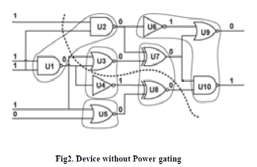
III. POWER GATING FOR DELAY REDUCTION: |
 |
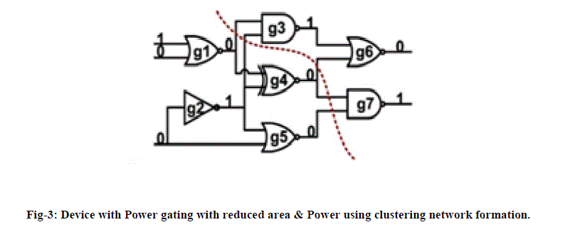 |
| This work presented a logic clustering based solution to the problem of controlling/optimizing the power gating parameters. The key design considerations in the power mode transitions are minimizing the wakeup delay, the peak current, and the total Size of sleep transistors. This work analyzed the relations between the three parameters, and solved the problem of finding logic clusters and their wakeup schedule that minimize the wakeup delay while satisfying the peak current and performance loss constraints. |
  |
  |
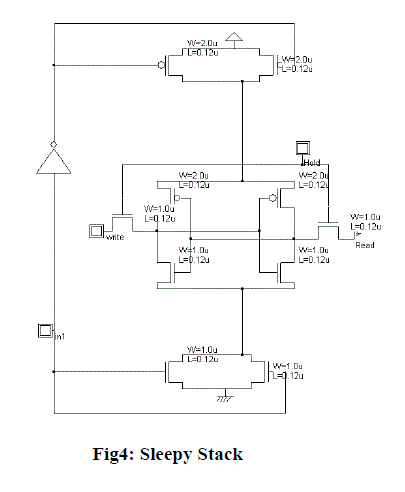
| A variation of the sleep approach, the zigzag approach, reduces wake- up overhead caused by sleep transistors by placement of alternating sleep transistors assuming a particular pre-selected input vector [4]. Another technique for leakage power reduction is the stack approach(Fig.4), which forces a stack effect by breaking down an existing transistor into two half Size transistors [5]. The divided transistors increase delay significantly and could limit the usefulness of the approach. |
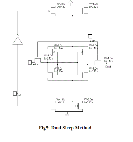
| The sleepy stack approach (Fig. 5) combines the sleep and stack approaches [2, 3]. The sleepy stack technique divides existing transistor into two half Size transistors like the stack approach. Then sleep transistors are added in parallel to one of the divided transistors. During sleep mode, sleep transistors are turned off and stacked transistors suppress leakage current while saving state. Each sleep transistor, placed in parallel to the one of the stacked transistors, reduces resistance of the path, so delay is decreased during active mode. |
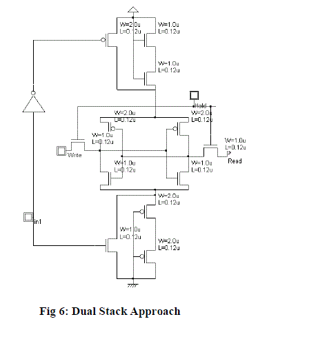
| However, area penalty is a significant matter for this approach since every transistor is replaced by three transistors and since additional wires are added for S and S’, which are sleep Signals. Another technique called Dual sleep approach [11] (Fig. 6) uses the advantage of using the two extra pull- up and two extra pulldown transistors in sleep mode either in OFF state or in ON state. Since the dual sleep portion can be made common to all logic circuitry, less number of transistors is needed to apply a certain logic circuit. |
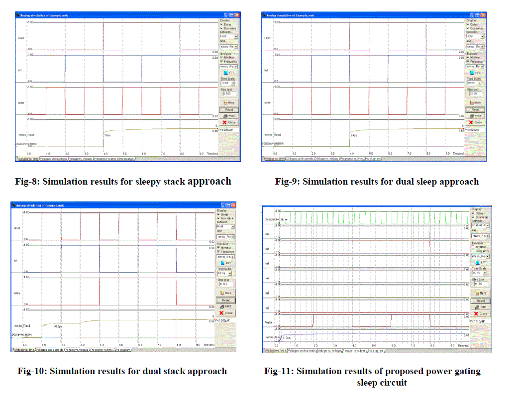
V. SIMULATION RESULTS |
 |
VI. CONCLUSION |
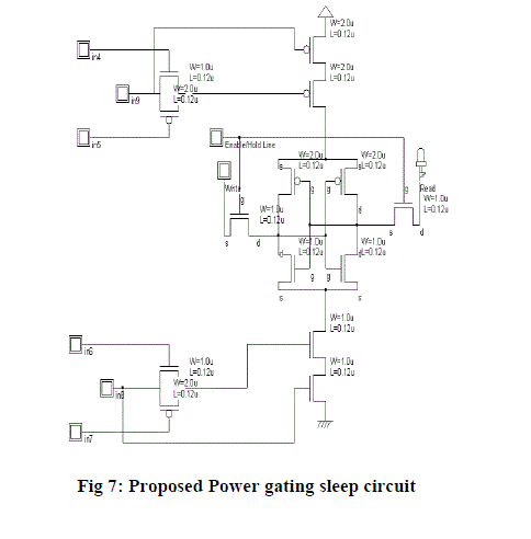
| In nanometer scale CMOS technology, sub threshold leakage power consumption is a great challenge. Although previous approaches are effective in some ways, no perfect solution for reducing leakage power consumption is yet known. Therefore, designers choose techniques based upon technology and design criteria. In this paper, we provide novel circuit structure named “Dual stack” as a new remedy for designer in terms of static power and dynamic powers. The Dual stack approach shows the least speed power product. Therefore, the dual stack technique provides new ways to designers who require ultra-low leakage power consumption with much less speed power product. Especially it shows nearly 50-60% of power usage than the existing digital power gating circuits. So, it can be used for future integrated circuits for reducing power consumption. If we implement this power gating technique to other reaming circuits, we may identify the drastic decrease in power consumption. It may be the great advantage of power gating technique. |
References |
|