International Journal of Advanced Research in Electrical, Electronics and Instrumentation Engineering
ISSN ONLINE(2278-8875) PRINT (2320-3765)
ISSN ONLINE(2278-8875) PRINT (2320-3765)
Nisarg Shah1, Bijeev N.V.2, Vasant Jani3, V.K. Jain4
|
| Related article at Pubmed, Scholar Google |
Visit for more related articles at International Journal of Advanced Research in Electrical, Electronics and Instrumentation Engineering
This paper explains Field-programmable gate array (FPGA) based digital control of DC-DC phase shifted full bridge converter operating at very high switching frequency. To achieve required high switching frequency, theoretically very high clock frequency is needed but how to achieve with less clock frequency has been shown here. The implementation in FPGA includes control algorithm and hybrid Digital Pulse Width Modulator (DPWM). Microsemi’s Proasic3E FPGA is used for implementation with 32 MHz clock frequency to achieve required 1 MHz switching frequency.
Keywords |
| Field-programmable gate array (FPGA), Digital Pulse Width Modulator (DPWM), Sigma-Delta (Σ - Δ) modulator. |
I. INTRODUCTION |
| Digital control of Switch-mode power supplies (SMPS) operating at high frequency are very useful and attractive because of significant improvement in power supply circuit characteristic. The advantages of using digital control includes low influences of external variation at input, realization using very few external passive components, handling of design tool is easy and so fast implementation is possible, control and power management techniques are advanced but is simple to understand, programmability, easy to change design without actual hardware being changed, ease of integration with digital system. The conventional analog control used in such case offers dynamic response which depends on the operating point and typically, SMPS feedback loops are designed which works on linear small-signal models to get desired performance at the nominal operating point [1] but with this flow we have to initially design the flow of an analog controller for dc–dc power converter and that usually requires knowledge of its control-to output transfer function, in order to achieve proper stability margins and dynamic closed-loop performances [2]. Also with this flow the behavior of passive and active component under different condition such as temperature variation, component tolerance variation, frequency of operation has to be taken into consideration. |
| To overcome with the disadvantage of the analog control flow, the recent methodology become attractive in all the types of field is digital control. Because of the large number of advantages including low sensitiveness to the variation in the input, ease of use i.e digital design tool comes with simple operation, advanced control strategy and the most important is re-programmability to check behavior at different input-output task without being changed the actual hardware [3], digital controller has become an attractive candidate for high-frequency dc–dc converters [4]. Also because of the large advantages it is possible to consider different design and verification tool for different design which leads to improve the performance of closed- loop response for dynamic operation, reduce the design time and so the improved robustness of SMPS [1] which again can be helpful to use as high-performance SMPS in portable electronic applications [4], where the most common demand is to miniaturize the system and for that the reduction in size of component is achieved with high switching frequency [3]. |
| The present implementation in this field is using the PI compensator for the phase shifted full bridge converter topology which is shown in [16]. Also here the development is done using the DSP development board for the different load configuration. The implementation for the forward DC-DC Converter is done using the different method of generating the PWM pulses in [3] with the FPGA based implementation. |
| There are various ways by which we can do the digital controlled operation such as using Microcontroller, DSP, ASIC, FPGA etc. Keeping in mind the advantages and disadvantages of available choices, the method to be selected as a final selection in such a way that it gives more appropriate and desired result for the application where we intended to apply that. Out of the above mentioned choices, the Field-Programmable-Gate- Array (FPGA) based controllers for highfrequency; digitally controlled SMPS [4] is creating noticeable interest for getting the best appropriate result for the application with the help of more efficient and correct development tools [5]. The FPGA embedded systems development represents a significant technological advantage to migrate from microprocessors, micro-controllers and Digital Signal Processors (DSP), which are more conventionally used in SMPS [5]. |
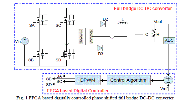
| FPGAs available to us for any of the applications are of three kinds – SRAM type, Flash type and Antifuse type each with its own associated advantages. Fig. 1 shows a block diagram of FPGA based digitally controlled buck converter with phase shifted full bridge converter topology. The major modules to look inside in the digitally controlled blocks are ADC, Control algorithm and DPWM. |
 |
| In general there are various topologies of buck converter but out of the available topologies this paper focused on phase shifted full bridge converter based DC-DC Converter. The paper is organized as follows. Section II is explains operational principle. Section III details the control algorithm. Section IV emphasize on the selection of DPWM architecture. And finally section V shows the main result of this paper. |
II. BASIC PRINCIPLE OF OPERATION |
| Fig. 1 shows FPGA based digitally controlled buck converter’s operational block diagram. The ADC will convert the output voltage of full bridge converter and gives the digitized value after sampling according to ADC selected. This value is then compared with the fixed reference signal and gives error signal as an output. This error signal will be considered as an input to duty command generator block. The control algorithm block is the duty command generator block and it will give the duty command according to the error signal after processing. The DPWM block is the block which gives the required PWM pulse for switching the MOSFET switches. For the full bridge converter, the required 4 PWM pulses are having a kind of nature that switch A and B as well as switch C and D is 180âÃÂð out of phase, switches A and D as well as switches B and D is of same phase. The DPWM block takes the duty command as an input, generated by control algorithm block and gives the PWM pulses at the switching period required by MOSFET switches. |
III. CONTROL ALGORITHM |
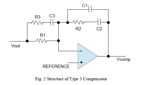
| In The main function of control algorithm block is to design a compensator which generates the duty command from the error signal. Basically main two types of control are there one is voltage mode and the other is current mode control. Here the voltage mode control has been selected for the forward converter. The type of compensator is three: Type 1, Type 2 and Type 3. Out of the three choices available, Type 3 has been selected and its structure is shown in Fig. 2. |
 |
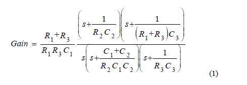
| The gain of the type 3 in s domain is [6], |
 |
| This equation in S-Domain has to be converted into discrete domain by means of conventional method available to convert such as Pole zero method, Impulse invariance method. Using matched pole zero method of transformation, z= esT, the equation of gain in discrete time is of the form of |
 |
| Where, k1, k2, k3, k4, k5, k6 are the coefficients, y(n) is output at nth instant, and likewise for n – 1, n – 2 and n – 3, same way x(n – 1) is input at (n – 1)th instant and likewise for n – 2 and n – 3.This equation is to be implemented in Verilog language for the FPGA realization. |
IV. DPWM ARCHITECUTRE |
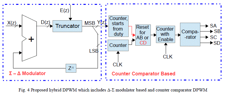
| Spectrum DPWM generates the PWM pulses required to drive the MOSFET switch with the duty command generated by control law at its input. The resolution of DPWM should be at least one bit higher than the resolution of ADC to avoid limit constraint [7]. In general there are various kind of DPWM architecture are available such as hardware architectures: Counter comparator DPWM [8], delay line DPWM [9], segmented delay line DPWM [10], Hybrid DPWM [11], and soft methods: Digital dither DPWM [12], sigma delta DPWM [13] etc. |
| Counter comparator are simple to construct but the major problem comes when the resolution of DPWM is increased because the clock frequency of N-bit resolution DPWM at switching frequency fs is 2N *fs. So if the SMPS switches at high frequencies, then the clock frequency required will be too large which in fact cause the high power consumption. Delay line DPWM and a segmented Delay line have some series of delay cell and that takes the clock frequency as switching frequency but area requirement is increase as the resolution increases. Hybrid DPWM is a combination of counter comparator and delay line DPWM as a compromise of power consumption and area requirement. Digital Dither and sigma delta DPWM are useful when very high resolution is required and as these both are soft methods; there is not a problem of area or power consumption. |
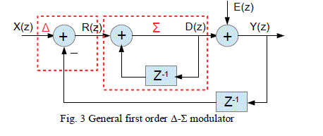
| The Δ-Σ DPWM is used to increase the resolution of DPWM without increasing the clock frequency. The Fig. 3 is the general first order Δ-Σ modulator. The Δ-Σ operation is based on the well known noise-shaping concept which is used in analog-to-digital and digital-to-analog converters [14], [15]. The Δ-Σ modulator sometimes also works as error feedback filter for DPWM. |
 |
| Although the Δ-Σ noise-shaping modulator is not new in IC design for ADC, it has not yet been widely used in recent digital PWM control. Till now, two Δ-Σ DPWM modulators have been proposed in digitally controlled low power high-frequency SMPS [11] with first-order and second-order Δ-Σ DPWM. |
| In this paper we have proposed the hybrid DPWM with the combination of the first-order Δ-Σ DPWM and counter comparator DPWM. The proposed hybrid DPWM architecture is shown in Fig. 4. |
 |
V. RESULT |
| The FPGA used in the prototype is Microsemi’s (Actel) ProAsic3E family’s A3PE1500.The code is written in one of the HDL language Verilog and simulation software being used is Libero IDE v9.1 software and MATLAB for analog part of compensator design. |
| The compensator transfer shown in (1) is implemented in MATLAB with the component values as follow: R1 = 4.12 kΩ, R2 = 20.5 kΩ, R3 = 150 Ω, C1 = 0.22 nF, C2 = 2.7 nF, C3 = 6.8 nF. With the mentioned component value the bode plot of compensator design in MATLAB is shown in Fig. 5. |
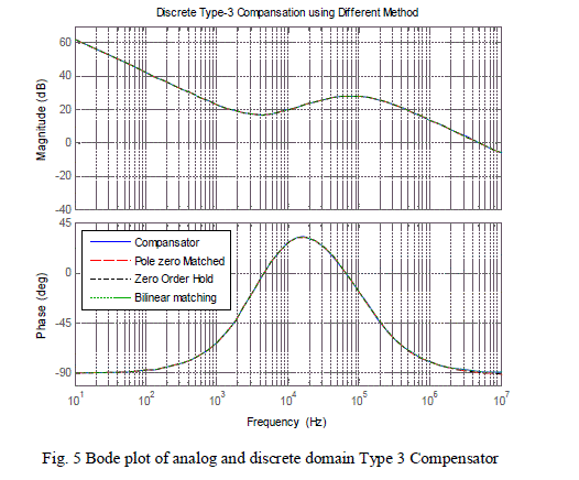 |
| From the fig. 5 it is visible that the compensator analog response is correctly matched with the discrete response of bilinear transformation as compared with the other transformation. The transformation method available to convert from analog to discrete transformation are Pole zero matching, zero–order hold and the bilinear transformation. From [16] it is found that the phase shifted full bridge with digital control simulated for the PI Controller which is replaced here by the Type 3 Compensator in order to achieve phase boost of 180 degree which may be beneficial for the application where the phase boost is required and not the gain modification. After simulation in MATLAB, the discrete transform is available and then we can get it in discrete time domain of the eq |
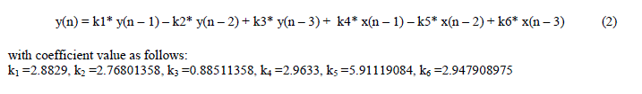 |
| This equation is implemented with coefficient values as mentioned above in Verilog language. |
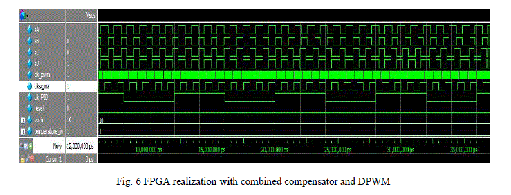 |
| Fig. 6 shows the simulation of FPGA realization in Microsemi’s Proasic3E family’s A3PE1500 FPGA prototype and the Software used is Libero IDE v9.1 from the FPGA manufacturer. The desired switching frequency of 1 MHz is achieved at the clock frequency of 32 MHz at 11 bit DPWM resolution using hybrid DPWM. To avoid the limit cycle constraint, DPWM resolution is 11 bit because the selected ADC is of 10 bit resolution. Reference voltage is 1 V. In the Fig. 6, SA,SB,SC,SD are the switching PWM pulses to be applied at all four MOSFET switches of phase shifted full bridge converter and the duty cycle is changing with input duty command from compensator. |
VI. CONCLUSION |
| The PWM pulses of all four MOSFET switches of phase shifted full bridge converter with desired fs of 1 MHz is achieved using only 32 MHz fclk at 11 bit resolution of hybrid DPWM, a combination of Δ-Σ and counter comparator DPWM and the duty cycle is varying based on duty command. |
ACKNOWLEDGMENT |
| This paper and related research is supported by the Space application center - Indian space research organization (SACISRO), Gujarat, India. I, Nisarg Shah thankful to all the Employees and persons associated with my division, and Nirma University, Gujarat for giving me an opportunity to work in the India’s best research organization. |
References |
|