International Journal of Advanced Research in Electrical, Electronics and Instrumentation Engineering
ISSN ONLINE(2278-8875) PRINT (2320-3765)
ISSN ONLINE(2278-8875) PRINT (2320-3765)
Anjali Menon1, R.Madhumitha2
|
| Related article at Pubmed, Scholar Google |
Visit for more related articles at International Journal of Advanced Research in Electrical, Electronics and Instrumentation Engineering
This paper presents the designing of a low powered (25-30 watts), portable and cost effective solar micro-inverter wherein the single solar panel is able to run the AC loads along with DC loads. The system consists of a solar panel, DC-DC push-pull converter, DC-AC inverter, LC filter and the test loads. The solar cell powers DC-DC push pull converter which boosts the input DC voltage into the desired rated input voltage of the inverter. The ripple is reduced by using a pi filter between the converter and inverter circuits. High frequency Pulse Width Modulated (PWM) pulses are generated by a microcontroller (PIC) and provided to the switches of half bridge inverter. The 220V PWM sine wave output of the inverter is conditioned to pure sine wave by an L-C filter. The performance of closed loop system is also evaluated.
Keywords |
| Inverter, Photovoltaic (PV), PWM, Solar. |
I.INTRODUCTION |
| Electricity generated from sunlight is called solar electricity and the process of converting solar light into electricity is known as the photovoltaic process. In this process direct current (DC) electricity is produced. DC power needs heavy cables to transform or transmit and suffer significant losses [5]-[6]. The energy produced by photovoltaic process can solve the power crisis experienced by developing nations [2]. Majority of the electrical appliances work in 220V AC [3]. A solar micro–inverter is designed such that the 12V dc input of solar panel is converted into 220V AC. It is named “MICRO-INVERTER” because these inverters are meant to be embedded and integrated with the PV panel reducing overall system cost. |
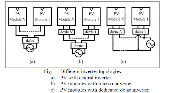
| The switch-mode power converters are widely used in PV energy conversion systems. Conventional installations where large PV arrays are connected to centralized power converters (Fig. 1(a)) are giving way to distributed architectures [1]. In one such architecture, dc/dc converters (micro converters) realize MPPT algorithms for individual PV modules. A central inverter converts the dc voltage sourced by a series string of such modules to mains-compatible ac voltage (Fig. 1(b)). Another architecture(Fig.1(c)). couples each PV module with a dedicated dc/ac inverter, commonly called as micro inverter [12]. Each module produces power at ac-mains voltage, and the central inverter is not needed. Fig.1 shows the different inverter topologies. |
 |
II. RELATED WORK |
| The paper [7] deals with designing of a single phase sine wave inverter .This system used eight solar panels ,each having 40W rated power. |
| The paper [12] deals with the solar inverters for grid application using a resonant inverter at input and a cycloconverter at the output side. |
| This paper is based on a previous research done at Independent University Bangladesh (IUB) [4] in which a solar home system was designed with solar panel of 30W power. |
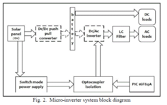
| In order to reduce cost and switching losses a modified model is proposed. The proposed system consists of a solar panel, DC-DC push-pull converter, DC-AC inverter, LC filter and the test loads. Battery is also provided to store charge during daytime. The solar panel supplies the DC voltage needed to activate the DC-DC push pull converter. The push-pull converter is directly connected to the switches of the half bridge circuitry. The DC-DC push pull converter boosts the input DC voltage into the desired rated input voltage of the inverter. High frequency Pulse Width Modulated (PWM) pulses are generated by a microcontroller (PIC) and provided to the switches of half bridge connection. The half bridge inverter outputs a PWM sine wave which is conditioned to pure sine wave by an L-C filter. The simulation results are obtained for multiple loads. |
III.METHODOLOGY |
| A pure sine wave has to be generated from the inverter to run AC loads (e.g. Table Fan). Square wave or modified sine wave inverters exist in the market but are very costly and have problems associated with performance[8]. In order to lower costs, a method of generating pure sine wave with Pulse Width Modulation (PWM) has been implemented [7]. However, one of the pre-requisites for using PWM is that the source voltage is larger than the output voltage .This introduces the need for a DC-DC converter which can provide the inverter with a high voltage source [9] Because the desired output of the inverter is 220 volts RMS, the DC-DC converter must supply 312 volts consistently. So the first step is to design a suitable DC-DC converter. |
| There are many methods of making a DC-DC converter [10]. For the model explained in this paper, most of them were not applicable because they were unable to operate in desired power range. The push pull converter has 85% efficiency at 350 watts of power. It also has a 50% duty cycle and isolates the input from the output through a double winding transformer [11]. The push pull converter works similar to that of the half bridge converter. The Half-Bridge Push-Pull Converter belongs to the primary switched converter family since there is isolation between input and output. |
| The PWM pulses and their complements are fed to the switches of the half bridge circuit. The output of the push pull converter (i.e. 312 volts) is the input to the half-bridge inverter circuit. A pi filter is connected to reduce the ripple in the output of the converter circuit. |
| The output of the inverter circuit is a sine wave with a switching frequency of 20 KHz. Here, the output sine wave is not pure due to harmonic generation in the inverter. An L-C filter is attached to the inverter which is connected in parallel to the load, which removes the unwanted harmonics and produces pure sine wave [7]. In the conventional converter circuit the output voltage contains ripples. A pi filter is included in the proposed circuit of the converter. This pi filter is designed by the equation (1) for ripple calculation |
| r = 1/ (4√2ω³LC²R) (1) |
| The block diagram of the solar micro-inverter system is shown in Fig.2. |
 |
IV. BLOCK DESCRIPTION |
| A. DC/DC Push Pull Converter |
| The 12V DC (Output of solar panel) is converted into 312V DC. To obtain an output of 220V AC from the inverter we have to give inverter an input of √2 times of 220V i.e, 220 * √2 ≈ 312 V. |
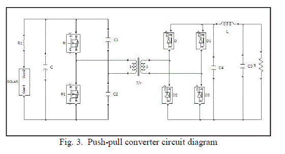 |
| As stated earlier, a push-pull converter is used for DC-DC conversion purpose. The turns ratio of the push pull transformer is calculated to be 1:53 turns. Fig.3. above shows the SIMULINK schematic that was used to simulate the output of the DC-DC converter. The output of the DC-DC converter is expected to be 312V DC. |
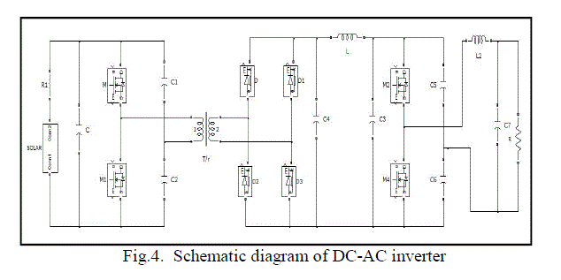
| B. DC/AC Inverter |
| The AC load needs pure sine wave 220V AC. So we need to convert 312V DC into 312V AC. Fig.4 shows the SIMULINK schematic that was used to simulate the output of the DC-AC inverter. The output of the DC-AC inverter is expected to be a 220V AC rms, 50 Hz sine wave. In order to eliminate the switching frequency and all multiples of the switching frequency, a low-pass filter needs to be inserted after the output of the full-bridge inverter. The cutoff frequency can be set by the formula (2) below |
| F cutoff =1/(2π√LC) (2) |
| The harmonics are located at the switching frequency and multiples of the switching frequency. The switching frequency is set at 20 KHz so that it would be distant from the 50 Hz fundamental frequency. This would allow a high cutoff frequency, which, by equation(2), allows for small LC components. The large distance between the harmonics and the fundamental frequency allows a large margin of error in the filter values. An L-C low-pass filter is designed for the power inverter. |
 |
V.SIMULATION MODELS AND RESULTS |
| To anticipate the outcomes of the micro-inverter, the parts of the whole system individually simulated and justified to the desired output values in SIMULINK. The system is simulated with R load, RL load, battery charging load and motor load. The closed loop analysis is also performed and the results are validated with the theoretical data. |
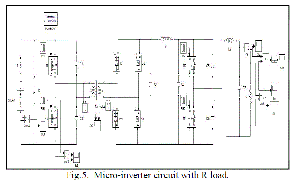
| A. Micro-Inverter Circuit With R Load |
| Fig.5 shows the circuit of a solar micro inverter with R load. |
 |
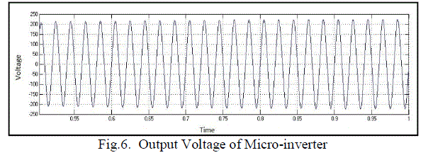
| The output voltage of the micro inverter is shown in Fig.6. and it is observed to be 220V at the load terminals. |
 |
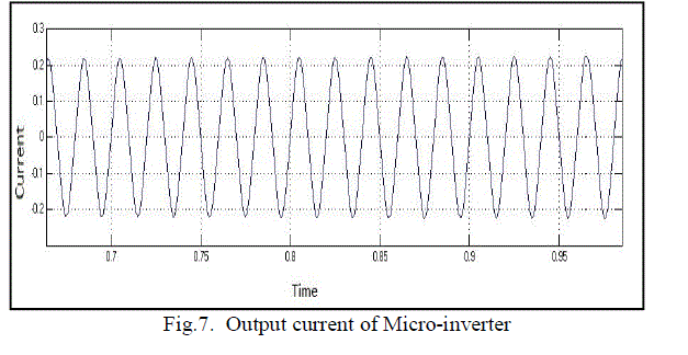
| The output current is shown in Fig.7 and it is observed to be 0.21 amperes. |
 |
| B. Harmonic Reduction |
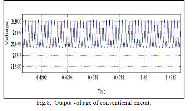
| The outputs of conventional and proposed push pull converters are compared. |
| A. Conventional Push Pull Converter Output : |
| Fig.8. shows the output of the conventional circuit. |
 |
| B. Proposed Push Pull Circuit Output : |
| Fig.9 shows the output of the proposed converter. |
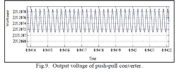 |
| Comparison of the two outputs shows that the conventional circuit had voltage ripple in the order of 0.11V whereas in the proposed circuit the ripple has been reduced to the order of 0.0008V. |
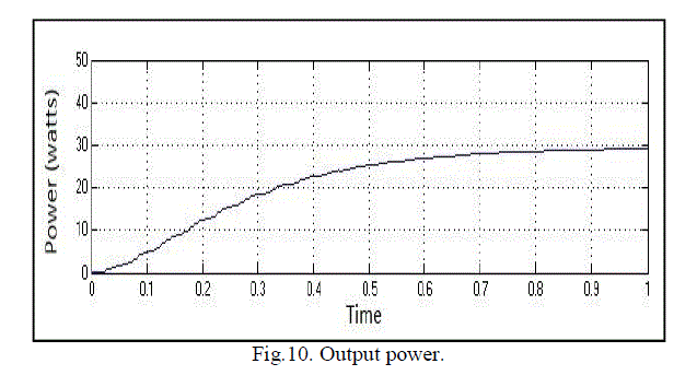
| C. Micro-inverter Circuit With RL Load |
| The Micro inverter with RL load shown in Fig.10. may be used for relay applications. The output power of the system is around 30W. |
 |
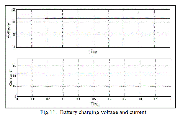
| D. Micro-Inverter for Battery Charging |
| The converter circuit can be used for battery charging which may be used during night time. The pi filter reduces the voltage ripple to 0.004V.The battery charging voltage and current waveforms are shown in Fig.11. |
 |
| E. Micro-Inverter With Motor Load |
| The micro inverter with motor load gives the output speed and torque waveforms are shown in Fig.12. |
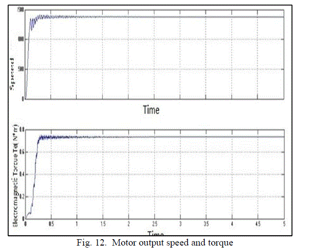 |
| The motor speed is observed to be around 1470 rpm, and the motor torque is around 0.74 Nm |
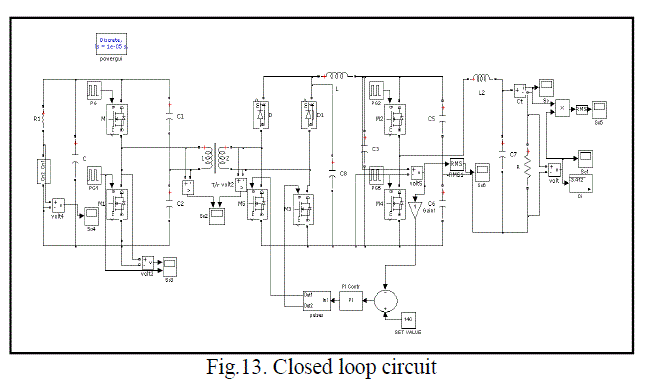
| F. Micro-Inverter ( Closed Loop action) |
| Let us consider that the disturbance in the circuit produces a surge in the output current .The desired current is 0.21A but due to the disturbance the output current is 0.29A. The micro-inverter circuit for closed loop action is shown in Fig.13. The output voltage is compared with a set value and the error is fed to the PI controller which controls the gating pulse of the rectifier circuit. |
 |
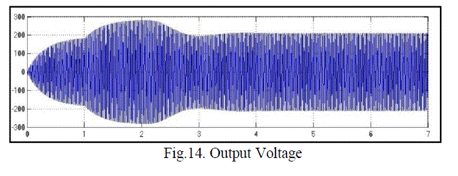
| The output voltage for the closed loop circuit is shown in Fig.14. |
 |
| The output current with the control action is shown in Fig.15. |
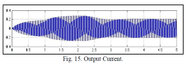 |
| The output voltage is set at 220V which is obtained at the output terminals after closed loop action and the output current is obtained as 0.21A as desired. |
VI.CONCLUSION |
| This paper has presented Design and Simulation of a Solar Micro-Inverter with Multiple Outputs. Simulation results are obtained with R load, RL load, Battery charging load and Motor load. |
| A closed loop analysis is also performed and the simulation results obtained shows a good agreement with the theoretical analysis. The steady state error is reduced by using PI controller. |
VII.FUTURE SCOPE |
| The closed loop system may be simulated using PID controller. The closed loop results with fuzzy controller may be compared with PI based system results. |
| The hardware will be implemented in the future. |
References |
|