Keywords
|
| Prescaler, Dynamic logic, E-TSPC, Frequency synthesizer, high speed digital circuit and WLAN |
INTRODUCTION
|
| Wireless LAN (WLAN) in the multi gigahertz bands, such as HIPER LAN II and Network standards like a 802.11a/b/g, are recognized as leading standards for high-rate data transmissions, and standards like Network protocol 802.15.4 are recognized for low-rate data transmissions. . The integrated synthesizers for Wireless LAN applications at 5 GHz reported in and consume up to 24 mw in CMOS realizations, where the first-stage divider is implemented using an Injection-locked divider which consumes large chip area and has a narrow locking range.The best published frequency synthesizer at 5 GHz consumes 9.6 mw at 1-V supply, where its complete divider consumes power around 6 mw, where the first-stage divider is implemented using the source-coupled logic (SCL) circuit, which allows higher operating Frequencies but uses more power. Dynamic latches are faster and consume less power compared to static dividers. |
| High speed divide-by- counter (also called prescaler) is a fundamental module for frequency synthesizers. Its design is crucial because it operates at a higher frequency and consumes higher power consumption. A divide-by- counter consists of flip-flops (FF) and extra logic, which determines the terminal count. Conventional high speed FF based divideby counter designs use current-mode logic (CML) latches [1] and suffer from the disadvantage of large load capacitance. This not only limits the maximum operating frequency and current-drive capabilities, but also increases the total power consumption. Alternatively, FF based divide-by designs adopt dynamic logic FFs such as true-single-phase clock (TSPC) [2]–[4]. The designs can be further enhanced by using extended true-single-phase-clock (E-TSPC) FFs for high speed and low power applications [5]– [10]. E-TSPC designs remove the transistor stacked structure so that all the transistors are free of the body effect. They are thus more sustainable for high operating frequency operations in the face of low voltage supply. Past optimization efforts on prescaler designs focused on simplifying the logic part to reduce the circuit complexity and the critical path delay. For example, an E-TSPC design embedded with one extra P-MOS/N-MOS transistor can form an integrated function of FF and AND/OR logic [7]. Moving part of the control logic to the first FF to reduce unnecessary FF toggling yields another version of prescaler design [8].These two classic designs each contains 16 transistors only and the mode control logic uses as few as 4 transistors. To achieve such circuit simplicity, it calls for a rationed structure in the FF design. Despite its distinct speed performance, the incurred static and short circuit power consumptions are significant. Latest designs presented in [10] adopt a general TSPC logic family containing both rationed and ratio less inverter alternatives. Since the maximum height of transistor stacking is up to 5, these designs lose their performance advantages when working under a low scenario. In [11], a power gating technique by inserting an extra PMOS between and the FF is employed in two novel divide-by-2/3 counter designs. The unused FF can be shut down when working in the divide-by-2 mode. Due to the increase in the number of transistor stacking (up to 4), these designs are not suitable for low operations. Due to the quadratic dependence of power consumption on supply voltage, lowering is a very effective measure to reduce the power at the expense of speed performance. .In particular, here focus on low operations for power saving without sacrificing the speed performance. In this design, rationed E-TSPC FFs are employed due to its circuit simplicity and speed performance. Only one pass transistor is needed to implement the mode control logic. The proposed design in capable of working at a maximum frequency of 531 MHz when the supply voltage is as low as 0.6 V. |
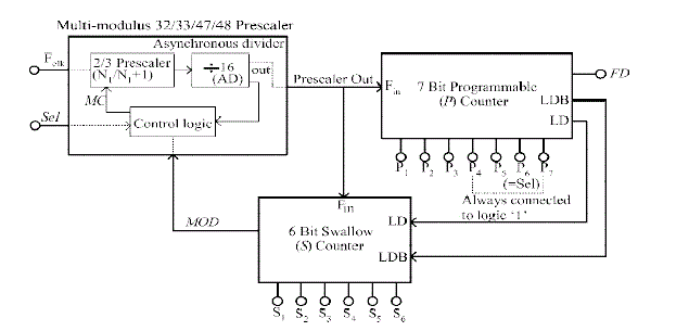
| The TSPC and E-TSPC designs are able to drive the dynamic latch with a single clock phase and avoid the skew problem. However, the adoption of single-phase clock latches in frequency dividers has been limited to PLLs with applications below5 GHZ.The frequency synthesizer reported in [6] uses an E-TSPC prescaler as the first-stage divider, but the divider consumes around 6.25 mw. Most Network protocol 802.11a/b/g frequency synthesizers employ SCL dividers as their first stage, while dynamic latches are not yet adopted for multiband synthesizers. In this paper, a dynamic logic multiband flexible integer-N divider based on pulse-swallow topology is proposed which uses a low-power wideband 2/3 prescaler and a wideband multi modulus 32/33/47/48 prescaler as shown in Fig. 1. The divider also uses an improved lowpower loadable bit-cell for the Swallow-counter. |
DESIGN CONSIDERATIONS
|
| The key parameters of high-speed digital circuits are the propagation delay and power consumption. The maximum operating frequency of a digital circuit is calculated and is given by |
 (1) (1) |
| The total power consumption of the CMOS digital circuits is determined by the switching and short circuit power. The switching power is linearly proportional to the operating frequency and is given by the sum of switching power at each output node as in |
 (2) (2) |
| Where n is the number of switching nodes, fclk is a clock frequency CLi is the load capacitance at the output node of the ith stage, and Vddis the supply voltage. Normally, the short-circuit power occurs in dynamic circuits when there exists direct paths from the supply to ground which is given by |
 (3) (3) |
| The short-circuit power is much higher in E-TSPC logic circuits than in TSPC logic circuits. However, TSPC logic circuits exhibit higher switching power compared to that of E-TSPC logic circuits due to high load capacitance. For the ETSPC logic circuit, the short-circuit power is the major problem. The E-TSPC circuit has the merit of higher operating frequency than that of the TSPC circuit due to the reduction in load capacitance, but it consumes significantly more power than the TSPC circuit does for a given transistor size. |
WIDEBAND E-TSPC 2/3 PRESCALER
|
| The E-TSPC 2/3 prescaler consumes large short circuit power and has a higher frequency of operation than that of TSPC 2/3 prescaler. The wideband single-phase clock 2/3 prescaler used in this design do not consist of two D-flip-flops and two NOR gates embedded in the flip flops as in Fig. 2. The first NOR gate is embedded in the last on DFF1, and the second NOR gate is embedded in the first stage of DFF2. |
MULTTMODULUS 32/33/47/48 PRESCALER
|
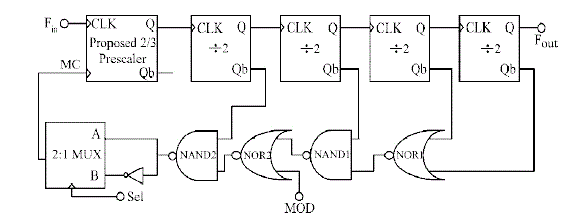
| The proposed wideband multi modulus prescaler which can divide the input frequency by 32, 33, 47, and 48 is shown in Fig.2. It is similar to the 32/33 prescaler but with an additional inverter and a multiplexer. The -proposed prescaler performs additional divisions (divide-by-47 and divide-by-48) without any extra flip flop, thus saving a considerable amount of power and also reducing the complexity of multi band divider. |
| A. Case 1: sel='0' |
| When sel='0', the output from the NAND2 gate is directly transferred to the input of 2/3 prescaler and the multi modulus prescaler operates as the normal 32/33 prescaler, where the division ratio is controlled by the logic signal MOD. If MC=I, the 2/3 prescaler operates in the divide-by-2 mode and when MC=O, the 2/3 prescaler operates in the divide-by-3 mode. If MOD=I, the NAND2 gate output switches to logic "I" (MC=I) and the wideband prescaler operates in the divideby- 2 mode for entire operation. The division ratio N performed by the multi modulus prescaler is |
 (4) (4) |
| Where N =2 and AD=16 is fixed for the entire design. If MOD=O , for 30 input clock cycles MC remains at logic "1", where wideband prescaler operates in divide-by-2mode and, for three input clock cycles, MC remains at logic "0" where the wideband prescaler operates in the Divide-by-3 mode. The division ratio N+ 1 performed by the multi modulus prescaler is and |
 (5) (5) |
| When sel=' 1', the inverted output of the NAND2 gate is directly transferred to the input of 2/3 prescaler and the multi modulus prescaler operate as a 47/48 prescaler, where the division ratio is controlled by the logic signal MOD. If MC= 1, the 2/3 prescaler operates in divide-by-3 mode and when MC=O,The 2/3 prescaler operates individe-by-2 mode which is quite opposite to the operation performed when sel='O' If MOD=I, the division ratio N+ 1 performed by the multi modulus prescaler is same except that the wideband prescaler operates in the divide by-3 mode for the entire operation given by |
 (6) (6) |
| If MOD=I, the division ratio N performed by the multi modulus prescaler is |
 (7) (7) |
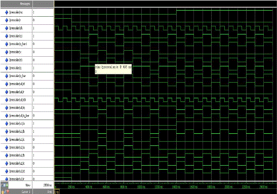
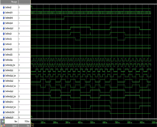
| The proposed multi modulus 32/33/47/48 Prescaler operation diagrams are shown on the above Figure. |
MULTIBAND FLEXIBLE DIVIDER
|
| It consists of Multimodulas 32/33/47/48 prescaler, a 7-bit programmable counter and 6-bit swallow counter. Here the prescaler is briefly discussed in the section. The control signal SEL decides whether the divider is operating in lower frequency band (2.3 GHZ) or higher band (5-5.75 GHZ). |
| A. Swallow (S) Counter |
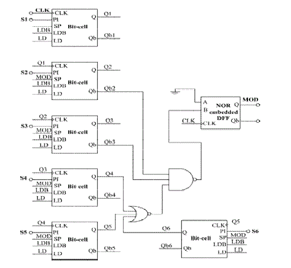
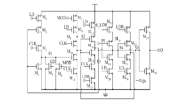
| The 6-bit s-counter consists of six asynchronous loadable bit-cells, a NOR-embedded DFF and additional logic gates to allow it to be programmable from 0 to 31 for low-frequency band and from 0 to 47 for the high-frequency band. The asynchronous bit cell used in this design shown in Fig.4. Is similar to the bit-cell except it uses two additional transistors M6 and M7whose inputs are controlled by the logic signal MOD. If MOD is logically high, nodes S 1 divide-by- 48) and P, S counters start down counting the input clock cycles. When the S-counter finishes counting, MOD switches to logic "1" and the prescaler changes to the divide-by-n mode (divide-by-32 or divide-47) for the remaining P-S clock cycles. |
| B. Programmable (P) Counter |
| The programmable P-counter is a 7-bit asynchronous down counter which consists of 7 loadable bit-cells and additional logic gates. Here, bit P7 is tied to the Sel signal of the multi modulus prescaler and bits P 4 and P7 are always at logic "1." The remaining bits can be externally programmed from 75 to 78 for the lower frequency band and from 105 to 122 for the upper frequency band. When the P-counter finishes counting down to zero, LD switches to logic "1" during which the output of all the bit-cells in S-counter switches to logic "1" and output of the NOR embedded DFF switches to logic "0" (MOD=O) where the programmable divider get reset to its initial state and thus a fixed division ratio is achieved. |
CONCLUSION
|
| In this paper demonstrated that pass transistor logic system has considerable implementation. It is proposed for power reduction. The operations of Multimodulasprescaler are according to their modes of operation. Here the input frequencies are divided into multiple ranges while the power consumption is reduced. A Multimodulasprescaler are verified and multiband flexible divider is verified. In this project provides solution to the low power, PLL synthesizer is implemented. The proposed multiband flexible divider consumes power 52 mw. In future work, we are going to reduce the power consumptions and achieve maximum operating frequency and also reducing the complexity of the circuits using pass transistor logic. Since the Multimodulas 32/33/47/48 prescaler has maximum operating frequency of 6.2 GHz, the values of P- and S-counters can actually be programmed to divide over the whole range of frequencies from 1 to 6.2 GHz with finest resolution of 1 MHz and variable channel spacing. However, since interest lies in the 2.3- and 5–5.725-GHz bands of operation, the P- and S-counters are programmed accordingly. |
| The proposed multiband flexible divider also uses an improved loadable bit-cell for Swallow S-counter and consumes a power of 0.96 and 2.2 mw in 2.3- and 5-GHz bands, respectively, and provides a solution to the low power PLL synthesizers for Bluetooth, Zigbee, Network standards’ 802.15.4, and 802.11a/b/g Wireless LAN applications with variable channel spacing. |
Figures at a glance
|
 |
 |
 |
 |
| Figure 1 |
Figure 2 |
Figure 3 |
Figure 4 |
|
 |
 |
 |
 |
| Figure 5 |
Figure 6 |
Figure 7 |
Figure 8 |
|
References
|
- V. K. Manthenaet al., “A 1.8-V 6.5-GHz low power wide band single phase clock CMOS 2/3 prescaler,” in IEEE 53rd Midwest Symp. CircuitsSyst., Aug. 2010, pp. 149–152.
- P. Y. Deng et al., “A 5 GHz frequency synthesizer with an injection locked frequency divider and differential switched capacitors,” IEEETrans. Circuits Syst.I, Reg. Papers, vol. 56, no. 2, pp. 320–326, Feb.2009.
- L. Lai Kan Leung et al., “A 1-V 9.7-mw CMOS frequency synthesizer for IEEE 802.11a transceivers,” IEEE Trans. Microw. Theory Tech.,vol. 56, no. 1, pp. 39–48, Jan. 2008.
- V. K. Manthenaet al., “A low power fully programmable 1 MHz resolution 2.4 GHz CMOS PLL frequency synthesizer,” in Proc. IEEEBiomed.Circuits Syst. Conf., Nov. 2007, pp. 187–190.
- X. P. Yu et al., “Design and optimization of the extended true single phase clock- based prescaler,” IEEE Trans. Microw. Theory Tech., vol.56, no. 11, pp. 3828–3835, Nov. 2006.
- S. Shin et al., “4.2 mw frequency synthesizer for 2.4 GHz Zigbee application with fast settling time performance,” in IEEE MTT-S Int.Microw.Symp. Dig. , Jun. 2006, pp. 411–414.
- X. P. Yu et al., “Design of a low power wideband high resolution programmable frequency divider,” IEEE Trans. Very Large Scale Integer.(VLSI) Syst., vol. 13, no. 9, pp. 1098–1103, Sep. 2005.
- M. Alioto and G. Palumbo, Model and Design of Bipolar and MOS Current-Mode Logic Digital Circuits. New York: Springer, 2005.
- S. Vikaset al., “1 V 7-mw dual-band fast-locked frequency synthesizer,” in Proc. 15th ACM Symp. VLSI, 2005, pp. 431–435.
- S. Pelleranoet al., “A 13.5-mw 5 GHz frequency synthesizer with Dynamic-logic frequency divider,” IEEE J. Solid-State Circuits, vol. 39, no.2, pp. 378–383, Feb. 2004.
- J. M. Rabaeyet al., “Digital integrated circuits, a design perspective,” in Ser. Electron and VLSI, 2nd ed. Upper Saddle River, NJ: Prentice-Hall, 2003.
- H. R. Rategh et al., “A CMOS frequency synthesizer with an injected locked frequency divider for 5-GHz wireless LAN receiver,” IEEE J.Solid-State Circuits, vol. 35, no. 5, pp. 780–787, May 2000.
- Y. Ji-renet al., “A true single-phase-clock dynamic CMOS circuit technique,” IEEE J. Solid-State Circuits, vol. 24, no. 2, pp. 62–70, Feb. 1989.
|