International Journal of Advanced Research in Electrical, Electronics and Instrumentation Engineering
ISSN ONLINE(2278-8875) PRINT (2320-3765)
ISSN ONLINE(2278-8875) PRINT (2320-3765)
Nemili Suresh Reddy1, P. Mahesh Kannan2
|
| Related article at Pubmed, Scholar Google |
Visit for more related articles at International Journal of Advanced Research in Electrical, Electronics and Instrumentation Engineering
Now a day’s technology enhancement is at a blistering pace. Merely VLSI has a meteoric rise due to the adoption of new techniques. Static CMOS had a limitation of deploying constant power supply. Less power dissipation is an essential attribute for any optimized design. Varying the power supply is the very thing for preventing the power dissipation. An adiabatic logic is a new technique to reduce power dissipation. Barrel shifter is an important block in any computational hardware architecture. This paper gives a detailed account of 32 bit barrel shifter design using 3 techniques namely Differential Cascode Voltage Switch Logic( DCVSL), Differential Cascode voltage Switch Pass transistor Adiabatic Logic(DCVPAL), Complementary Pass transistor Adiabatic Logic(CPAL) and Positive Feedback Adiabatic Logic( PFAL). The analysis is carried out in Tanner spice and H-Spice using 180nm technology
Keywords |
| Power clock, DCVSL, DCVPAL, CPAL, PFAL, Power dissipation |
I. INTRODUCTION |
| Full-swing voltage-mode CMOS logic styles have been extremely successful both technically and in terms of market share. Switching power dissipation of CMOS circuit with capacitive load has a lower limit of CLVdd 2/2. Adiabatic logic circuits are a new form of circuits much different from static CMOS circuits. Obviously this circuits would be CMOS in nature but adiabatic CMOS[3]. The term “adiabatic” refers to the thermodynamic processes that exchange no heat with the environment. In adiabatic switching circuits the power dissipation is below the lower limit i.e, below CLVdd 2/2. Reduction of power dissipation occurs at the cost of slower speed of operation. It also allows the recycling of energy to reduce the total energy drawn from the power source so that these are also known as reversible logic circuits[4]. |
 |
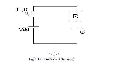 |
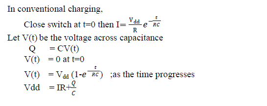
| Here as the time progresses IR voltage gradually come down because current gradually reduced and the Q/c voltage goes up as a result Vdd remains constant. |
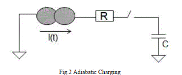 |
| 1. A time dependant current source, I(t) is used to charge the capacitance C. |
| 2. Above circuit is used to model a CMOS circuit with certain output resistance driving a capacitive load[7]. |
| 3. The load capacitance is not having any charge at time 0[4]. The voltage across the capacitance as a function of time, Vc(t), is given by : |
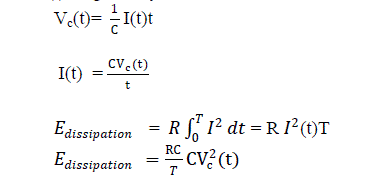 |
| 4. For T>2RC, the dissipated energy is smaller than the conventional case. i.e, when T>2RC the energy dissipation becomes half of CV2 so that the power dissipation is reduced. |
| 5. The dissipation can be made arbitrarily small by further extending the charging time T. |
| 6. The dissipated energy is proportional to R; a smaller R results in a lower dissipation unlike conventional case[4]. |
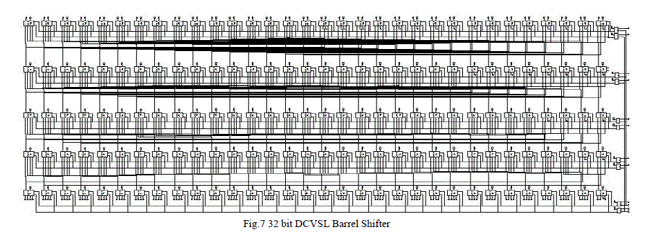
II. BARREL SHIFTER |
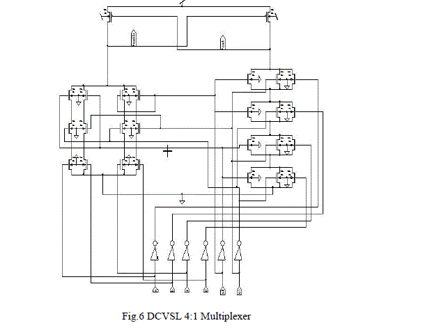
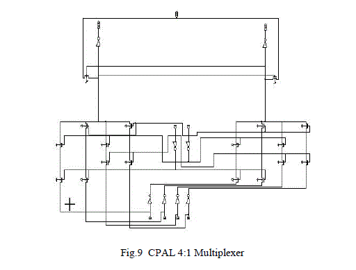
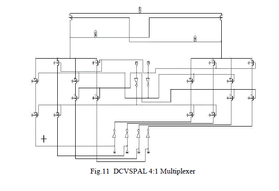
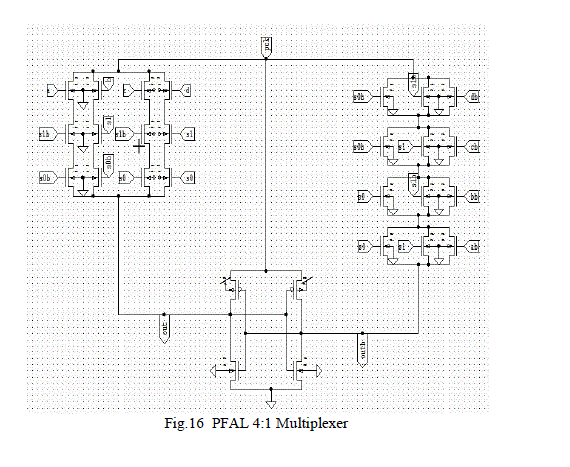
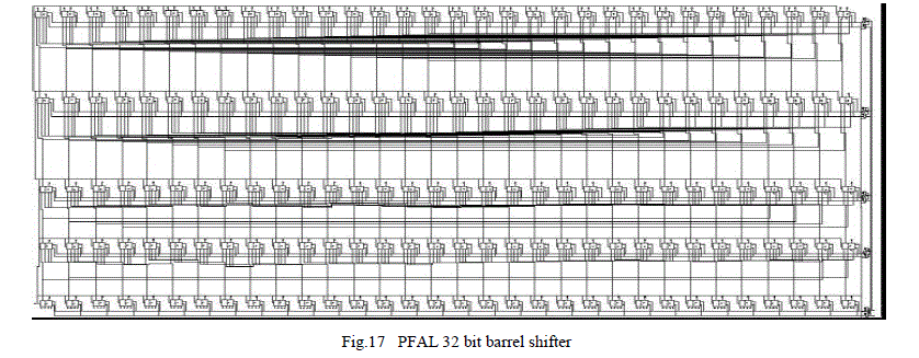
| Barrel shifter is one of the important computational blocks on hardware. Barrel shifter performs 3 type of shifting operations circular shift, logical shift and arithmetic shift. It is of two types mask based and multiplexer based[1]. In multiplexer based barrel shifter, selection lines are used for shifting controls[1]. Here barrel shifter design encompasses 4:1 multiplexers and 2 input and gates. |
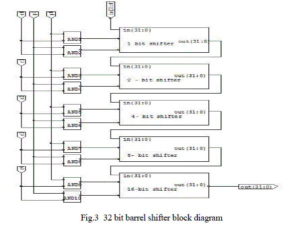 |
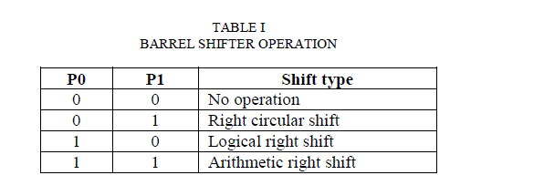
| Above figure gives the pictorial representation of 32 bit barrel shifter. Here p0, p1 and c(4:0) ensures the type of shift among 3 shifts. In(31:0) is the value to be shifted c(4:0) is the number of bit positions to be shifted. The output of two and gates work as selection lines to the multiplexers. Here we use 4:1 multiplexers |
 |
III. DIFFERENTIAL CASCODE VOLTAGE SWITCH LOGIC |
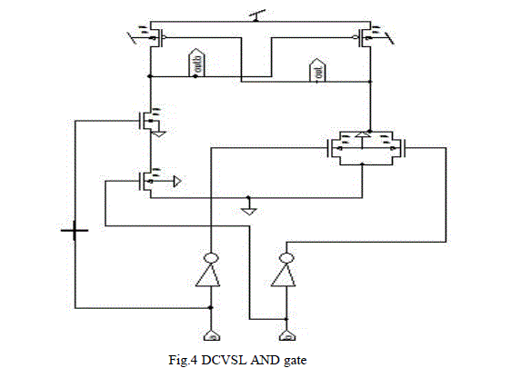
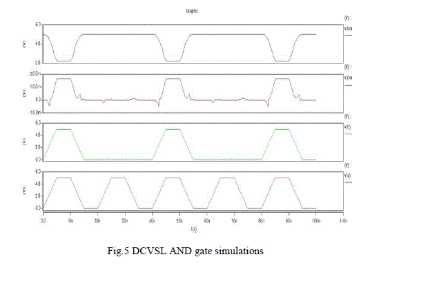
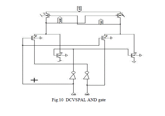
| Here pull up network consists of two PMOS transistors are connected back to back to back in the form of a latch[6]. Fig.3.1 is a schematic diagram for 2-input DCVSL AND gate. The pull down network performs the actual AND and NAND operation. operation. It gives complementary outputs. Here we use constant DC power supply. |
 |
 |
 |
 |
IV. ADIABATIC TECHNIQUES |
| A. Pass transistor logic design rules |
| 1. One must not drive the gate of a pass transistor by the output of another pass transistor else there is a degradation at the output level[6]. |
| 2. It is essential to provide both charging and discharging path for the load capacitance. |
| 3. Need to avoid simultaneous path to ground and Vdd. |
| B. Advantages of pass transistor logic |
| 1. Ratioless because the output does not dependant on the size of the NMOS and PMOS transistors. |
| 2. Lower area due to smaller number of transistors. |
| 3. Lesser power dissipation; no static power and short-circuit power dissipation. |
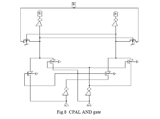
| C. CPAL and DCVPAL |
| In CPAL inverting buffers perform restoration of logic levels at the output. Inverting buffers allow driving large capacitive loads. The PMOS switch performs swing restoration. The PMOS transistors should be properly sized so that the circuit can function correctly[6]. Here we use ramped power clock as power supply instead of constant DC power supply for less power dissipation. |
| In DCVSPAL we use complementary outputs so that it is called dual rail logic. The PMOS latch performs the swing restoration and the time varying ramp is used as power supply instead of constant dc power supply but due to the floating output there is a power dissipation. |
 |
 |
 |
 |
 |
 |
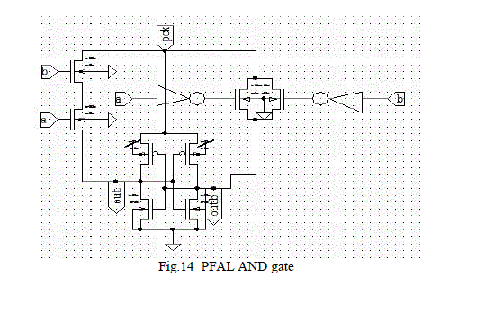
| D. PFAL |
| Here the input NMOS network is connected in parallel to the PMOS transistors. Here the back to back inverters are for providing feedback network which is used in the recovery phase to reduce power dissipation[2]. Here also we use complementary outputs i.e, dual rail logic. Here during charging mode the output load charges to Vdd but during discharging phase instead of going to ground the charge is recycled to the power-clock through the feedback network[2]. |
 |
 |
 |
 |
V. SIMULATION RESULTS AND ANALYSIS |
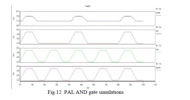
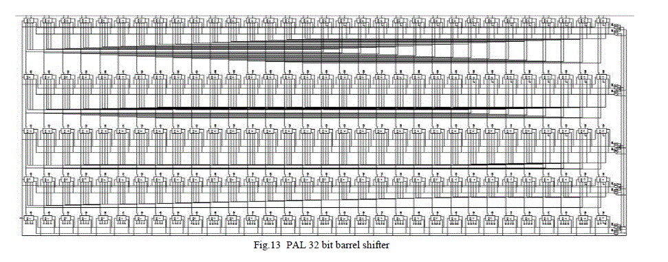
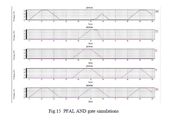
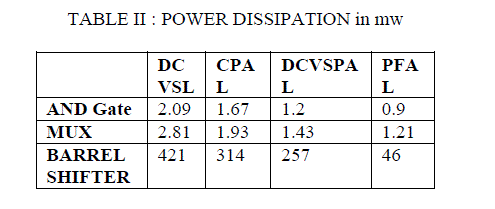
| To analyze the performance of the barrel shifter among 4 techniques and compare the adiabatic logic with static CMOS, the design and analysis is carried out in Tanner spice and H-Spice 180nm technology. We implemented 4:1 multiplexer and 2-input AND gate schematics in schematic mode of tanner and created the symbol for both. We deploy the symbols as instances in the barrel shifter design. Where as in pass transistor logic the delay is more because the signal has to pass through so delay is more in pass transistor logic the output doesn’t depend on the size of the transistors i.e, irrespective of size of the transistors it gives the output. Where as in PFAL which is more efficient among all 4 techniques gives the better performance in terms of power dissipation. Barrel shifter design consists of 160 multiplexers and 10 AND gates. |
 |
VI. CONCLUSION |
| Since, the adiabatic logic is an efficient technique for designing low power circuits in terms of power, delay and efficiency compared to conventional CMOS logic. From the analysis we can conclude that PAL and PFAL, both are efficient for designing the logic circuits but PFAL has an advantage over PAL for its modular design because PAL has a drawback of floating node and more delay so that PAL dissipate more power compare to PFAL. In PFAL there is there is no floating output so PFAL has better energy savings than PAL. These adiabatic techniques can be used to implement not only barrel shifter design but also for many arithmetic and logic circuit designs. |
ACKNOWLEDGMENT |
| Author would like to thank the Department of Electronics and Communication Engineering of SRM University to carrying the work successfully. |
References |
|