International Journal of Advanced Research in Electrical, Electronics and Instrumentation Engineering
ISSN ONLINE(2278-8875) PRINT (2320-3765)
ISSN ONLINE(2278-8875) PRINT (2320-3765)
Nemili Suresh Reddy1, P. Mahesh Kannan2
|
| Related article at Pubmed, Scholar Google |
Visit for more related articles at International Journal of Advanced Research in Electrical, Electronics and Instrumentation Engineering
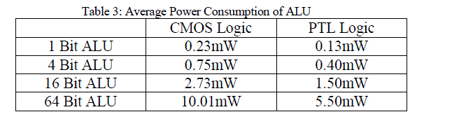
The main objective of this project is to design low power 64 bit ALU. Here ALU is designed with the help of multiplexers and full adder. The main component in the ALU is full adder. In CMOS method eight transistor full adder and CMOS based multiplexers are used. In PTL method six transistor full adder and PTL based multiplexers are used. To reduce area, ripple carry adder is used in ALU. Pass transistor logic is used to reduce the number of transistors by eliminating redundant transistors. Number of active devices in PTL logic is less compared to CMOS logic. By using less number of active devices, power consumption is reduced. By reducing area and by using PTL based multiplexers low power ALU is attained. In the implementation of ALU using PTL method, the power and area are reduced to 55% compared to CMOS method.
Keywords |
| 6TFA, 8TFA, ALU, CMOS Logic, Multiplexers, Pass transistor logic. |
I. INTRODUCTION |
| The Arithmetic Logic Unit is essentially the heart of a CPU. It has more applications in DSP and micro processors. In the past, VLSI designers concentrated more on area, performance, cost and reliability [1]. The least importance was given to power. Now a dayâÃâ¬ÃŸs power is given primary importance than area and speed. The two low power logic styles used in ALU are CMOS logic and PTL logic. Two important characteristics of CMOS logic are high noise immunity and low static power consumption. Since the one transistor of the complementary pair is always turned off. For high density logic functions CMOS logic is best. Pass transistor logic reduces transistor count by eliminating redundant transistors. By reducing transistors we can reduce area and then power. Here transistors are used as a switch to pass logic levels between nodes of a circuit, instead of connecting switches directly to supply voltages. This reduces number of active devices. With the increase in usage of portable devices, need for low power is increased greatly. Designers are always giving more importance to power rather than speed, because there is a reliability problem in high performance system. High performance systems often turns hot, and high temperature tends to exacerbate several silicon failure mechanisms. Every 10 degrees Celsius increase in operating temperature roughly doubles a component failure rate. From the environment point of view, the smaller the power dissipation of electronic systems, the lower the heat pumped into the rooms, the lower the electricity consumed and hence the lower the impact on global environment. There is always a tradeoff between power, area and delay. Depending upon requirement, the designer will selects the low power logic techniques. |
II. ALU DESIGN USING CMOS METHOD |
| A. Full adder Design |
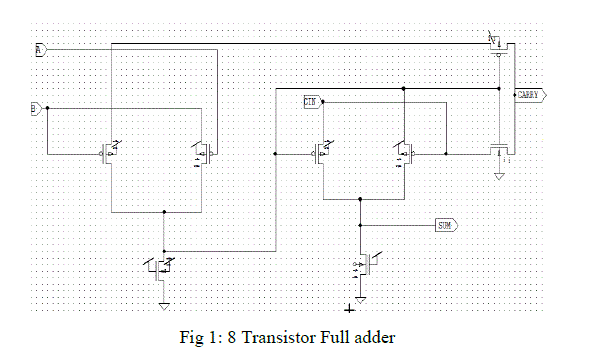
| The adder is one of the most important components of a CPU, Arithmetic logic unit (ALU) and address generation like cache. In addition, full-adders are important components in other applications such as digital signal processors (DSP) architectures and microprocessors. In the CMOS method 8 T full adder is used. Fig.1 shows the circuit level diagram of 8 T full adder [2]. Eight transistor Full adder is designed using two 3T XOR gates [5]. The Full adder inputs are three and the outputs of the Full adder are six namely, SUM, CARRY, AND, EXOR, EXNOR, OR. Additional OR circuit is used to perform OR operation. We can get EXNOR operation by giving output of EXOR to inverter circuit. Additional AND circuit was used to perform AND operation. |
| B. Multiplexer Design |
| The multiplexers have been used in the ALU design for input and output signal selection. In CMOS method multiplexer is designed using CMOS logic. Inputs to 4:1 multiplexer are logic1, logic0, B0 and B0âÃâ¬ÃŸ. S0 and S1 are select signals. Depending upon select signals input will be selected as output. In CMOS method multiplexers are designed with the help of CMOS logic. |
| C. ALU Design |
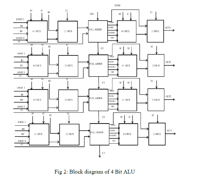
| ALU is designed by using 4x1 multiplexer, 2x1 multiplexer and Full adder. The input and output sections consist of 4x1 and 2x1 multiplexers and the main logic is implemented by using full adder. In the first design multiplexers and full adder are implemented using the CMOS logic. A set of three select signals have been used in the design to determine the operation being performed and the inputs and outputs being selected. Fig. 2 shows the block diagram of 4-bit ALU [4]. Ripple carry adder is used in ALU. Here the carry bit cascaded from input to output stage [1]. The 4-bit ALU consists of eight 4x1 multiplexers, four 2x1 multiplexers and four full adders. |
| The 4-bit ALU is designed in 180nm, n-well CMOS technology. For the INCREMENT operation logic „0âÃâ¬ÃŸ is applied as an input. For DECREMENT operation logic „1âÃâ¬ÃŸ applied as input. The complement of B is used for SUBTRACTION operation. The full adder performs the SUBTRACT operation by twoâÃâ¬ÃŸs complement method. An INCREMENT operation is analyzed as adding „1âÃâ¬ÃŸ to the addend and DECREMENT is seen as a subtraction operation [4]. |
 |
 |
III. ALU DESIGN USING PTL METHOD |
A. Full adder Design |
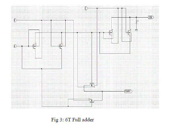
| In PTL method Full adder is designed using six transistors. Six transistor Full adder is designed using 2T XOR gate [3]. In PTL method two transistor XOR gates can be designed using general logic implementation. The circuit operation is as follows when A=0 and B=0 both the pmos transistors ON and it will produce the output low. When either one of the transistor is ON it produces output as high, when A=1 and B=1 both the pmos transistors are OFF and it will produces output as low. The six transistor Full adder is shown in the Fig.3 [3]. |
 |
| B. Multiplexer Design |
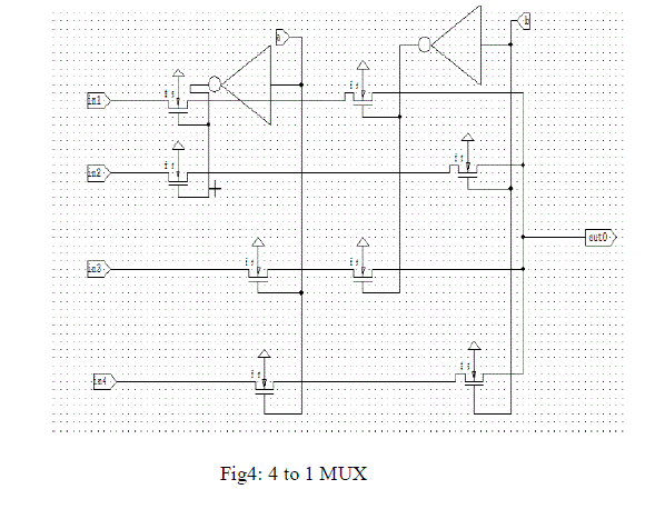
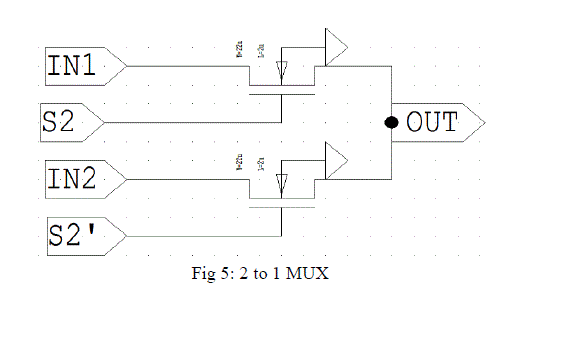
| Here the multiplexer is implemented using pass transistors. This design is simple and efficient in terms of area and timing. The pass transistor design reduces the parasitic capacitances and results in fast circuits. There are two kinds of multiplexers implemented: 2 to 1 multiplexer and 4 to 1 multiplexer. Schematic of 4 to 1 Multiplexer and 2 to 1 Multiplexer is shown in the Fig.4 [2] and Fig.5 [2] respectively. |
 |
 |
 |
| C. ALU Design |
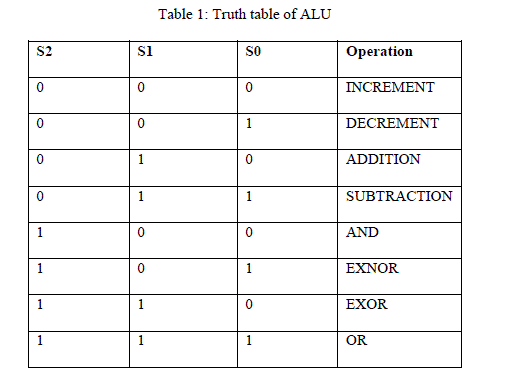
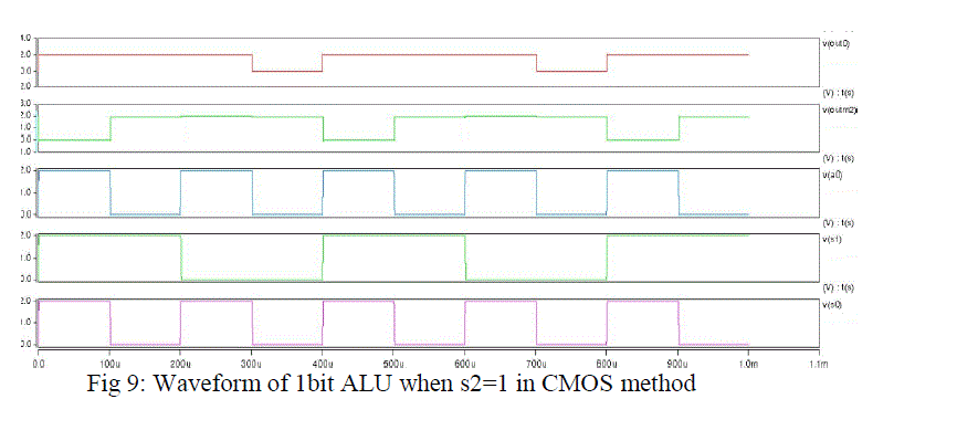
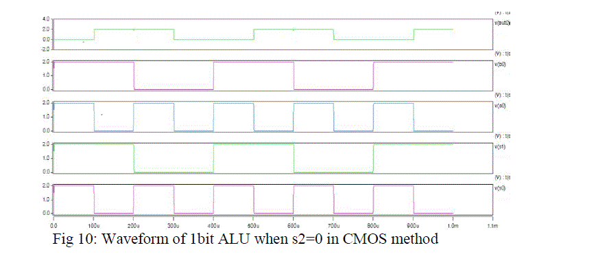
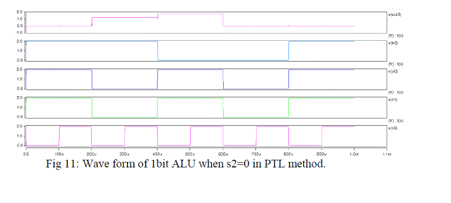
| Here ALU is designed using 6 transistor full adder and pass transistor logic based multiplexers. The pass transistor design reduces the parasitic capacitances and results in fast circuits. ALU operation depends upon select signals s0, s1 and s2. If s2=0 then it performs arithmetic operations. If s2=1 then it performs logical operations. The below Truth table gives the detailed explanation about ALU operation. Table 1 shows the Truth table of ALU. |
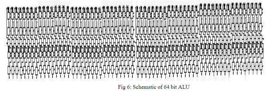
| 1) Schematic diagram of 64 bit ALU: The fig 6 shows the schematic diagram of ALU. Tanner Tool is used to draw the schematic of 64 bit ALU. |
 |
IV. RESULTS |
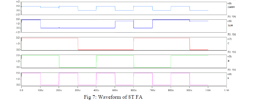
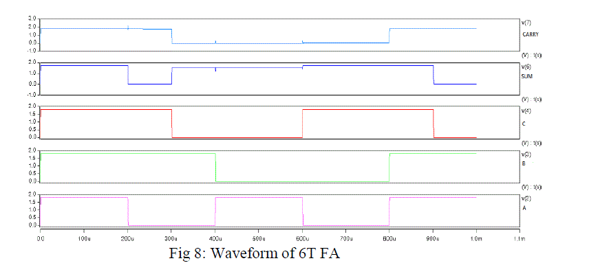
| The simulation of ALU design is done using HSPICE. The technology file used is tsmc018. Full adder inputs are A,B,C and outputs are sum and carry. |
 |
 |
 |
 |
 |
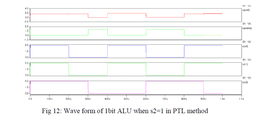 |
| I n ALU, Depending upon select signals S0, S1 and S2 operations will perform between A and B. |
 |
V. CONCLUSION |
| Average power consumed in 64 bit ALU using CMOS logic is 10.01mW and by using PTL logic power consumption has been reduced to 5.50mW. It is observed that the number of transistors in PTL method is less than CMOS method. So area reduced and then power also reduced. As shown in tabular diagram the average power consumption in PTL method is around 55% less than CMOS method. |
ACKNOWLEDGMENT |
| Author would like to thank the Department of Electronics and Communication Engineering of SRM University for carrying the work successfully. |
References |
|