International Journal of Advanced Research in Electrical, Electronics and Instrumentation Engineering
ISSN ONLINE(2278-8875) PRINT (2320-3765)
ISSN ONLINE(2278-8875) PRINT (2320-3765)
Jayalekshmi1, Vipin Thomas1
|
| Related article at Pubmed, Scholar Google |
Visit for more related articles at International Journal of Advanced Research in Electrical, Electronics and Instrumentation Engineering
In this paper, we present the design of a high frequency and low power analog to digital converter (ADC) which operates at 3V power supply using tsmc 0.18micron CMOS technology. The ADC designed is carried out by designing each building block of the circuit separately and then assembling them together to get the required ADC. The CMOS comparator, the digital to analog converter (DAC) and the successive approximation register (SAR) are the key elements in the design of the ADC. The CMOS operational amplifier was designed with a high unity gain frequency that will direct the ADC to operate at a greater speed. Design has been carried out in Tanner EDA tools. Simulation results are verified using S-edit and W-edit.
Keywords |
| CMOS, OPAMP, comparator, SAR, DAC |
I.INTRODUCTION |
| The contribution of signal processing as one of the major motivation to the fast development of electronic circuits is always worth mentioning. With the incredible advancement of modern VLSI technology, people are able to build more and more complex digital circuits on a single chip to realize signal processing that is traditionally achieved by analog circuits, because digital circuit has advantages over its analog counterpart in several aspects such as much lower noise sensitivity, excellent signal regenerating capability and it is easier to realize design and test automation as well. However, the object of signal processing originates in the fact that physical signals of the real world are always in analog form. Therefore, to facilitate the extensive DSP functions in the digital domain, interfaces between analog and digital blocks are omnipresent in all contemporary mixed signal processing integrated circuits. Analog to digital data converters are among the major components in the interfaces. TodayâÃâ¬ÃŸs trend in mixed-signal ASICs leads to integration of Analog-Digital-Converters (ADCs) with complex digital circuitry on a single chip. ADCs are a key element in mixed-signal ICs. |
| Wide applications such as wireless communications and digital audio and video have created the need for cost-effective data converters that will achieve higher speed and resolution. The needs required by digital signal processors continually challenge analog designers to improve and develop new ADC and DAC architectures. |
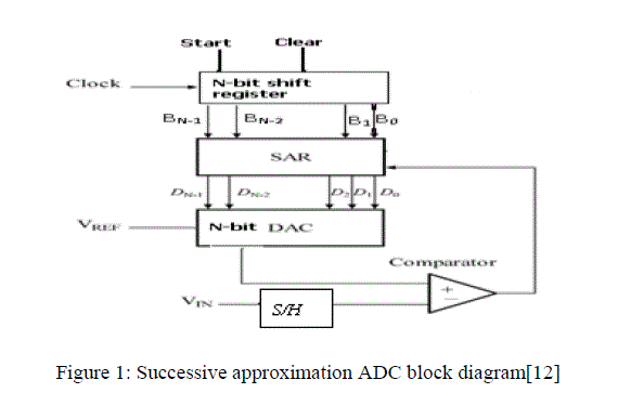
| Basically, the successive-approximation A/D converter, which is known for its very good power efficiency, consists of three main components-an analog comparator, a DAC, and a successive-approximation register (SAR), all of which are connected in a feedback arrangement as shown in Figure1. A more complete converter contains additional control logic for the CLOCK, CLEAR and START signals, and perhaps a set of data latches for the output bits. Because the SAR is the only digital network of the three, it has been one of the limiting factors in prior attempts to fabricate costcompetitive monolithic successive-approximation A/D converters since both analog and digital networks could not successfully be built on the same chip. Consequently, earlier attempts at a single-chip converter employed a dual-chip approach keeping the analog and digital portions of the converter on separate monolithic chips and then connecting on a single hybrid substrate [1]. |
| The work starts with designing a high frequency low power operational amplifier (OPAMP). An OPAMP is a DCcoupled high-gain electronic voltage amplifier with a differential input and, usually, a single-ended output. An op-amp produces an output voltage that is typically hundreds of thousands times larger than the voltage difference between its input terminals. OPAMPs are key elements in analog processing systems. Operational amplifier is the main bottleneck in our circuit. As shown in the figure 1, we need one DAC and Comparator circuit. OPAMP based DAC and comparator is implemented in the design of the analog to digital converter circuit. So design of high frequency low power OPAMP is the building block of the ADC circuit. |
 |
II.LITERATURE SURVEY |
| In a survey article on data conversion, it was pointed out that the most popular type of analog-to-digital (A/D) converter in use today is the one employing the successive-approximation (SA) algorithm [1]. The main reason for its popularity lies in its inherently fast conversion time which is a constant n clock periods for an n-bit converter. The successive approximation analog to digital converter, commonly known as SA-ADC - is widely used in industrial control applications and battery powered applications because of its good balance between speed and power consumption. When compared to other A/D schemes such as the dual-slope integrating method and the servo-type method, the successive-approximation scheme offers much higher conversion rates [2]. This is a highly desirable feature in multichannel data acquisition systems and in PCM telecommunication systems. The main disadvantage of this scheme has in the past been the dependency upon tight-tolerance often complex networks used in the implementation of the algorithm [3]. |
| Since design of high frequency and low power OPAMP is the key in our design, many papers in this field were also surveyed. In the approach by R.K Baruah [4], although the designed OPAMP worked at a low power and low voltage, but it presented a very low unity gain frequency. Miran Milkovic[5], explains the performance of high unity gainbandwidth current gain-based CMOS operational amplifiers fabricated in a 1.5-pm CMOS digital process is presented. High unity-gain bandwidth was achieved by using short-channel MOS transistors operating in the current gain mode. Stacked current mirrors have been utilized as current gain stages to minimize the effects of the channel-length modulation in short-channel MOS transistors. Although the simulation [6]done in HSPICE shows an operation at a low power supply and consumes lesser power, but still the increase that is observed in the unity gain frequency cannot be considered to be noteworthy. The research work [7] insists the incorporation of pseudo-cascode compensation instead of Miller compensation to increase the unity gain frequency up to 450MHz. But it is seen that this approach degrades the phase margin with the increase of unity gain frequency. Boaz Shem-Tov, Mücahit Kozak, and Eby G. Friedman [8] presented a method for the design of high speed CMOS Operational Amplifiers (Op-Amp). The Op-Amp consists of an Operational Transconductance Amplifier (OTA) followed by an output buffer. The OTA is compensated with a capacitor connected between the input and output of the buffer. The multi-stage design [9] improves the settling time and gain but leads to the decrease of the phase margin and unity gain frequency. Again, as the supply voltage decreases, it also becomes increasingly difficult to keep the transistors in saturation with the voltage headroom available [10]. Bhupendra K. Ahuja[11] described in detail how the commonly used two-stage CMOS operational amplifier suffers from two basic performance limitations due to the RC compensation network around the second gain stage. First, this frequency compensation technique provides stable operation for limited range of capacitive loads, and second, the power supply rejection shows severe degradation above the open-loop pole frequency. Moreover, in these procedures, the effect of capacitive load on unity gain frequency, speed, power and noise balancing altogether is not considered. In our work, an OPAMP has been designed which exhibits high unity gain frequency for optimized balancing of phase margin, gain, speed, power, noise and load. A method is proposed to set a higher unity gain frequency of the OPAMP working at a lower supply voltage. This allows the value of each circuit element of the amplifier (i.e transistor aspect ratios, bias current and compensation capacitor) to be univocally related to the required electrical parameters. |
III.THEORETICAL BACKGROUND |
| A. Principle of SA-ADC: |
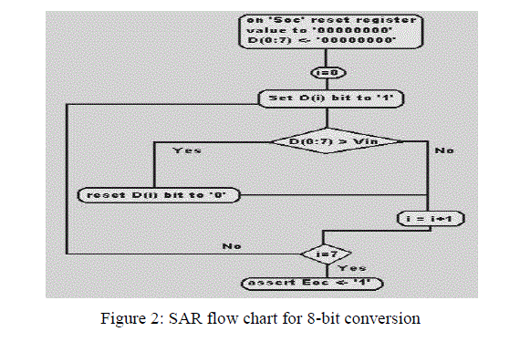
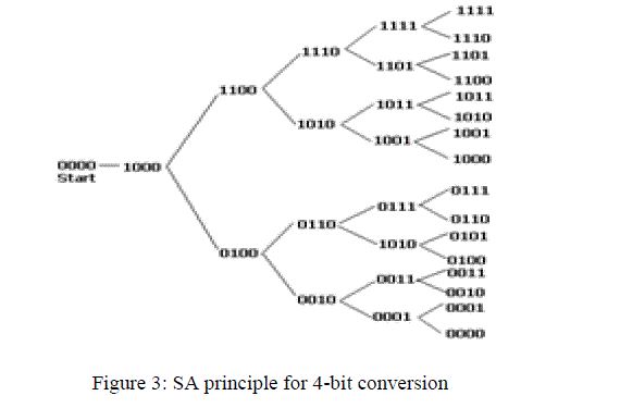
| The conversion process of a successive approximation A/D converter is basically a binary search through all possible quantization levels before converging on the final digital answer. This type of ADC operates by successively dividing the voltage range by half. An SA-ADC needs „nâÃâ¬ÃŸ steps to reach an accuracy of „nâÃâ¬ÃŸ bits, where each step comprises of three main operations- settling of DAC, comparator making a decision and control logic determining the next DAC level. |
| The MSB is initially set to „1âÃâ¬ÃŸ and the digital equivalent is compared with the unknown analog input voltage. If the DAC output is larger than the analog input voltage, then MSB stays „onâÃâ¬ÃŸ and the second MSB is also set to „1âÃâ¬ÃŸ i.e „onâÃâ¬ÃŸ state. Otherwise, MSB is reset to „0âÃâ¬ÃŸ or turned „offâÃâ¬ÃŸ state and the second MSB is set to „1âÃâ¬ÃŸ. This process is repeated down to LSB and by this time the converted digital value is available in the SAR. |
| The output of SAR is fed to the DAC whose output acts as the variable reference of the comparator, while the other input of the comparator is connected with the unknown analog input voltage. Here, the comparator output is used to approximate the unknown analog input voltage with the n-bit digital value of SAR. |
| The basic principle of this A/D converter is that the unknown analog input voltage has been approximated with a N-bit, digital value by trying one bit at a time, beginning with MSB. An N-bit register controls the timing of the conversion where N is the resolution of the ADC. Vin is compared to the output of the DAC. The comparator output controls the direction of the binary search, and the digital control is implemented using the successive approximation register (SAR) which holds the output code when the conversion is finished. |
| B. The algorithm: |
| The successive approximation algorithm is explained step-wise as follows with reference to figure 1[12]. |
| 1. A 1 is applied to the input to the shift register. For each bit converted, the 1 is shifted to the right 1-bit position. BN-1 =1 and BN-2 through B0 =0 |
| 2. The MSB of the SAR, DN-1, is initially set to 1, while the remaining bits DN-2 through D0 are set to zero. |
| 3. Since the SAR output controls the DAC and the SAR output is 100…0, the DAC output will be set to Vref/2. |
| 4. Next, Vin is compared to Vref/2. If Vref/2 is greater than Vin, then the comparator output is a 1 and the comparator resets DN-1 to 0. If Vref/2 is less than Vin, then the comparator output is a 0 and the DN-1 remains a 1. DN-1 is the actual MSB of the final digital output code. |
 |
| 5. The 1 is applied to the shift register is then shifted by one position so that BN-2=1, while the remaining bits are all 0. |
| 6. DN-2 is set to a 1, DN-3 through D0 remain 0, while DN-1 remains the value from the MSB conversion. The output of the DAC will now either equal Vref/4 (if DN-1=0) or 3Vref/4(if DN-1=1). |
| 7. Next, Vin is compared to the output of the DAC. If the DAC output is greater than Vin, the comparator the DN-2 is reset to 0. If Vin is less than the DAC output, DN-2 remains a 1. |
| 8. The process repeats until the output of the DAC converges to the value of Vin within the resolution of the converter. |
 |
| C. Operation of the SA-ADC: |
| In this design, instead of counting up in binary sequence, SAR counts by trying all values of bits starting with the mostsignificant bit and finishing at the least-significant bit. The SAR consists of a shift register and logic control units to control the output of the shift register in a particular sequence. Throughout the count process, the register monitors the comparator's output to see if the binary count is less than or greater than the analog signal input, adjusting the bit values accordingly. The advantage to this counting strategy is much faster results: the DAC output converges on the analog signal input in much larger steps than with the 0-to-full count sequence of a regular counter. |
| There are three distinct operations that are performed sequentially by an A/D converter: |
| (1) It samples a continuous-valued, continuous-time analog signal. |
| (2) It quantizes the sampled signal to a finite number of levels. |
| (3) It assigns a digital code to the related quantized level. |
| With this sequence of operations, any physical signal, no matter if it is mechanical, thermal, optical, acoustical, or magnetic, once it has been transformed into electrical signal by a proper sensor, it can be converted into digital signal by an A/D converter and processed conveniently with powerful digital signal processing components, out of which various useful information can be extracted. There are many research approaches to realizing the analog-to-digital conversion. As the continuation of this research, this work aims to design a circuit for the popular SA-ADC which will exhibit lower power consumption and requires a lesser conversion time, as the components incorporated, for example the analog comparator is one that has high speed of operation. |
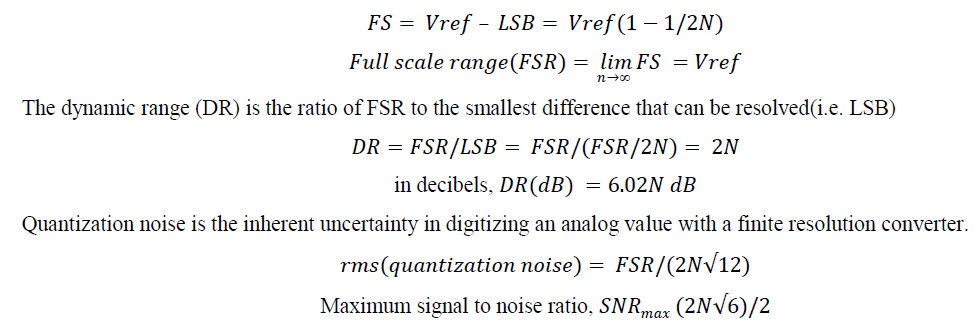
| The value of LSB is given by= Vref/2N |
| Again, the full scale (FS) is the difference between analog output for the largest digital word(111…) and the analog output for the smallest digital word(000…) |
 |
IV.DESIGN OF THE KEY COMPONENTS |
| A. The design of high frequency low power OPAMP: |
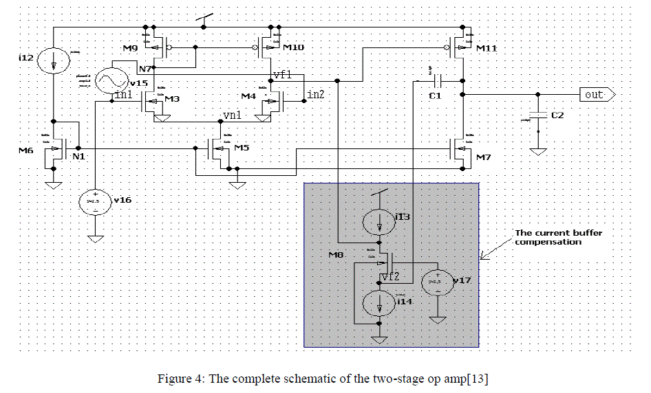
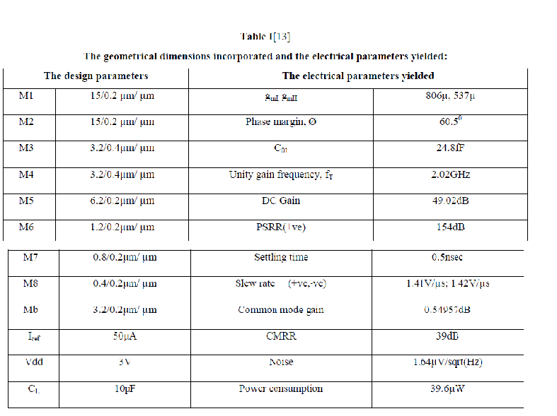
| OPAMP being a key element in an analog processing system, as proposed in our previous work [13], a high frequency CMOS operational amplifier (Op-Amp) shown in figure 4 which operates at 3V power supply using tsmc 0.18 micron CMOS technology was designed. As compared to the conventional approach, the proposed compensation method results in a higher unity gain frequency under the same load condition. The design parameters along with the electrical parameters yielded are as given in the table I. This circuit operates efficiently in a closed loop feedback system, with a current buffer compensation circuit while high bandwidth makes it suitable for high speed applications. The circuit operating conditions includes the room temperature as the operating temperature with a power supply of 3V and a load of 10pF. |
 |
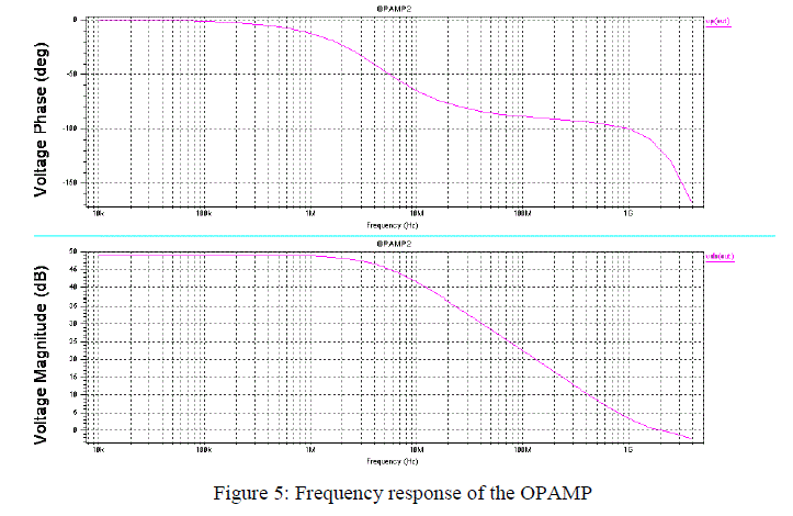
| For the frequency response plot, an ac signal of 1V is swept with 5 points per decade from a frequency of 10KHz to 4GHz. Fig.5 illustrates the frequency response which shows a dc gain in dB versus frequency in Hz (in log scale) and phase margin of OPAMP in open loop. The dc gain is found to be 49.02dB and phase margin 60.50 which is good enough for an OPAMP operating at a high frequency. A unity gain frequency of 2.02GHz is excellent for an OPAMP when all the other parameters are also set at an optimized value. |
 |
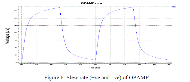
| The slew rate simulation is carried out performing a transient analysis using a pulse waveform of 1mV for a pulse period of 0.5nsec. The slew rate (+ve and –ve) are found to be 1.41V/μs and 1.42V/μs respectively, which is quite good as compared to other low power, low voltage OPAMPs. The slew rate response is as shown in figure 6. |
 |
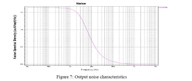
| The graph of output noise of the OPAMP is given below, yielding an output noise of 1.64μV/sqrt(Hz). |
 |
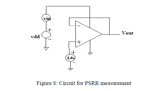
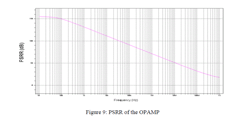
| The graph evaluating power supply rejection ratio (PSRR) in dB is shown in the following figure 9. PSRR measures the influence of power supply ripple on the OPAMP output voltage. It is the ratio of voltage gain from the input to output (open loop) to that from the supply to the output. PSRR can be calculated by putting the OPAMP in the unity gain configuration with the input shorted. The Miller compensation capacitance allows the power supply ripple at the output to be large enough. The PSRR (+ve) of the OPAMP in this design is calculated to be 154 dB . The circuit for PSRR calculation is shown below: |
 |
 |
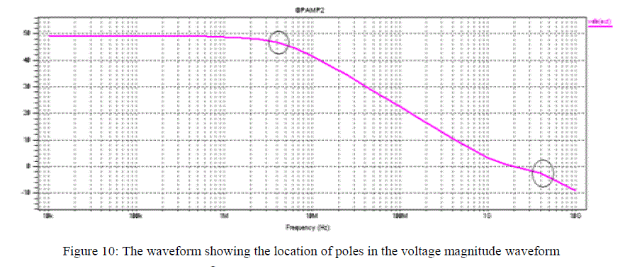
| The waveform below shows the location of the poles in the voltage magnitude waveform. |
 |
 |
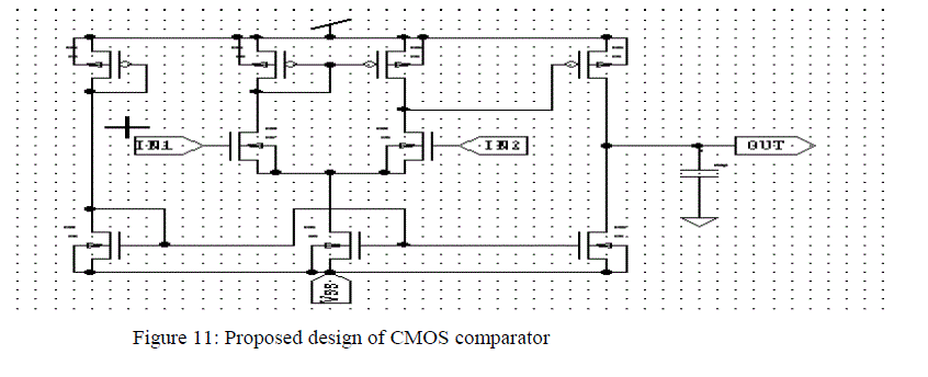
| B. CMOS comparator design: |
| The comparator is a circuit that compares an analog signal with another analog signal or reference and outputs a binary signal based on the comparison. The comparator design plays an important role in high speed ADCs. The function of comparison is a crucial, and often a limiting component in the design of high speed data conversion systems due to its finite accuracy, comparison, speed and power consumption. Using the same OPAMP of our previous work [13] with the same parameters , a comparator is designed which consists by using current mirrors, current sinks, active load & constant current source. Transistor W/L ratios are as selected which gives accurate & optimum results. Parasitic effects which influences in the comparators performance is minimized in this design. This help to get the desired output for a high speed & low power consumption. The comparator circuit is depicted in Figure 11 has been simulated using tanner tool with tsmc 0.18 micron CMOS technology. |
 |
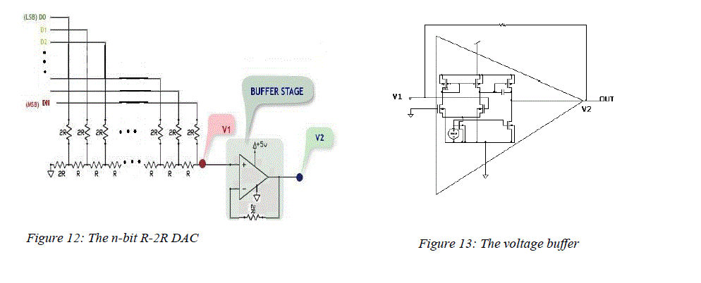
| C. Design of DAC: |
| A wide variety of DAC architectures exist, ranging from very simple to complex. Each has its own merits and demerits. Here, we have used the DAC architecture that incorporates fewer resistors and is called the R-2R ladder network. This configuration consists of a network of resistors alternating in value of R and 2R. Figure 12 illustrates an N-bit R-2R ladder. Starting at the right end of the network, the resistance looking to the right of any node to ground is 2R. Each node voltage is related to Vref by a binary weighted relationship caused by the voltage division of the ladder network. It uses resistors of only two different values, and their ratio is 2:1. An N-bit DAC requires 2N resistors, and they are quite easily trimmed. The total current flowing from Vref is constant, since the potential at the bottom of each switched resistor is always zero volts(either ground or virtual ground). Therefore, the node voltages will remain constant for any value of the digital input. In the voltage mode R-2R ladder DAC shown in Figure 12, the "rungs" or arms of the ladder are switched between Vref and ground, and the output is taken from the end of the ladder. The output may be taken as a voltage (V1). The voltage output has an advantage that is the constant output impedance which eases the stabilization of any amplifier connected to the output node. Additionally, the switches switch the arms of the ladder between a low impedance Vref connection and ground, which is also, of course, low impedance, so capacitive glitch currents tend not to flow in the load. On the other hand, the switches must operate over a wide voltage range (Vref to ground). This is difficult from a design and manufacturing viewpoint, and the reference input impedance varies widely with code, so that the reference input must be driven from a very low impedance. In addition, the gain of the DAC cannot be adjusted by means of a resistor in series with the Vref terminal. Figure 13 shows the CMOS circuit of the voltage buffer used in DAC. |
 |
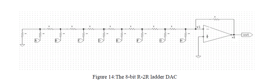 |
| As shown above in the figure 14 is an 8 bit DAC which is used in our design. |
| The SAR consists of a shift register and a control unit. |
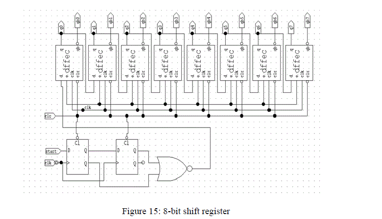
| D. Shift register: |
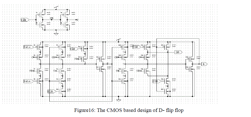
| In our work, Serial in Parallel out Register based SAR is used to design the ADC. Shift registers are a type of sequential logic circuit, mainly for storage of digital data. They are a group of flip-flops connected in a chain so that the output from one flip-flop becomes the input of the next flip-flop. Figure 15 shows the schematic of the shift register we used and the figure 16 shows the CMOS circuit of the D-flip flop that is used in the shift register. |
 |
 |
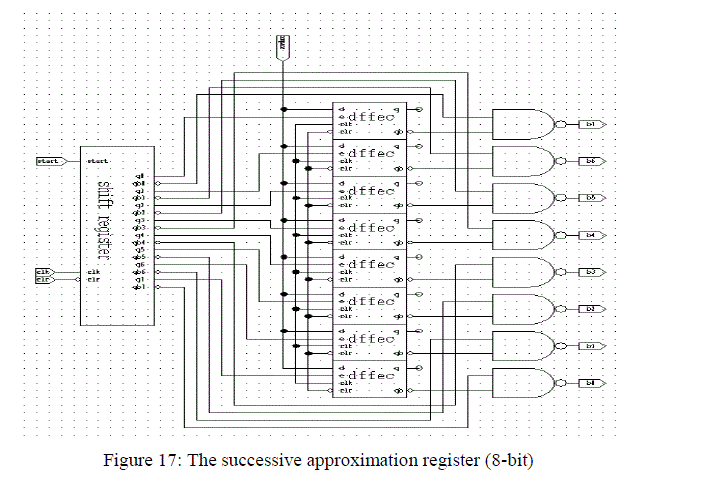
| E. The SAR control logic: |
| Of the several SAR designs presently in use, the most common design uses a separate sequencer and code register made from D-type flip-flops. The function of the sequencer (performed by the shift register) is to control the enable of the code register and sequentially setting each flip-flop in the register to a “trial” state such that on the next clock pulse, the flip-flop is conditionally set by the present information on the data line, i.e the data from comparator output. The advantage of this design lies in its simplicity and ease of layout which consists of reproducing each bit cell. The output of the shift register is fed to the enable input of the code flip-flop, while the complementary output of the shift register is fed as one of the input to the NAND gates. The complementary output of the code register is fed as the other input to the NAND gates. The comparator output is directly fed to the input of the code register which either sets or resets the output bits of the SAR in accordance to the binary search algorithm. The comparator output is compared with the bit at the clock when the particular code register is enabled. The output of the NAND gates provides the output of the SAR. The 8-bit SAR schematic is shown in the figure 17. |
 |
V. RESULT AND DISCUSSION |
| An 8 bit ADC is designed using the proposed method. The output waveform of the 8-bit SA-ADC is shown in figure 18. |
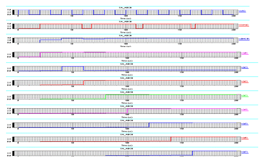 |
| Fig. 18: The output waveforms of a 8-bit SA-ADC |
| The whole conversion process is carried out in 8 clock cycles for the 8-bit SA- analog to digital conversion. The average power consumption in the conversion process is 2.4mW. The full scale(FS=Vref – LSB= Vref(1-1/2N) ) is 4.98. The dynamic range is 48.16dB. The rms quantization noise is 0.00564dB. The maximum signal to noise ratio is 313.5. |
VI.CONCLUSION |
| The primary goal of this work is to choose and optimize or develop an ADC topology with fast conversion time. For that purpose, a simple and fast successive approximation analog to digital converter design technique is proposed. Among the most conventional ADC, SA-ADC, that follows the principle of a binary search algorithm, have proven to exhibit a faster conversion and very efficient for the target resolution. The entire binary search in the ADC is based upon some digital logic that is implemented using the SAR, DAC and the comparator. These components are made up of flip flops and logic gates and are connected in a feedback manner. Successive approximation ADC is more suitable for interleaving. In this work, SA-ADC of 8-bits is designed, which can also be extended up to more number of bits. In the design, the only possible obstacle in high speed conversion is if the comparator had a limited gain-bandwidth product. But this difficulty is overcome with the use of the high speed comparator designed with the high frequency OPAMP. |
References |
|