International Journal of Advanced Research in Electrical, Electronics and Instrumentation Engineering
ISSN ONLINE(2278-8875) PRINT (2320-3765)
ISSN ONLINE(2278-8875) PRINT (2320-3765)
Karthika V L, Nimmy Sara George
|
| Related article at Pubmed, Scholar Google |
Visit for more related articles at International Journal of Advanced Research in Electrical, Electronics and Instrumentation Engineering
The fly-back converter is used in both AC/DC and DC/DC conversion with galvanic isolation between the input and outputs. More precisely, the fly-back converter is a buck boost converter with the inductor split to form a transformer, so that the voltage ratios are multiplied with an additional advantage of isolation. In the on-state the energy is transferred from the input voltage source to the transformer while the output capacitor supplies energy to the output load. In the off-state, the energy is transferred from the transformer to the output load and the output capacitor. By controlling the duty ratio of switch used in the primary of transformer a variable DC supply of zero to a designed maximum value is obtained. The switching signal is provided by programming a micro controller which provides a pulse width modulation. The control circuit is isolated using a optocoupler. A fly-back transformer is designed to meet the output requirement. In this project the aim is to design a pure DC supply that can be varied in the limit 0V to 44V from a fixed supply voltage of 12V, which is AC or DC. Thus DC output below 12V which is buck operation and DC output obtained above 12V which is boost operation is obtained. The variable voltage is obtained by adjusting the duty ratio of gate pulse of a MOSFET, which is connected to the primary of a fly-back transformer. The duty ratio is varied using a potentiometer.
Keywords |
| Fly back transformer, MOSFET, PIC, Optocoupler |
I. INTRODUCTION |
| In switch mode power supplies (SMPS), fly-back converters are very popular because of, design simplicity, low cost, multiple isolated outputs, high output voltages and high efficiency. They are preferred especially for low power applications. According to efficiency and power density, SMPSs are more popular than linear power supplies. Most of the advanced communications and computer systems require SMPS switch have high power density, high efficiency and constant operation frequency. |
| At the last decade, a lot of converter topology has been proposed for switch mode power supplies. Among the currently existing transformer coupled switching mode DC-DC converter, Fly-back converters are the simplest isolated DC-DC converter topology because of absence of inductor at the output filter, only one semiconductor switch and only one magnetic component transformer or coupled inductor. Besides, obtaining up to 5000V output voltage and having multiple outputs are the superiorities. Because of these advantages, fly-back converters become the most preferred DCDC converter topology for switch mode power supplies. |
| Fly-back converters are popular for its, simple in design for low power applications, Low cost because of less component 1requirement, Blocking voltage not occurred on the output diode, thus diode cost reduced, There is no additional inductor at the output circuit This simplifies the usage of multiple outputs, Transient response is fast because of output inductor absence. |
| Fly-back converters are preferred mostly for low power applications for low output power applications where the output voltage needs to be isolated from the input main supply. The output power of fly-back type SMPS circuits may vary from few watts to less than 100 watts. The overall circuit topology of this converter is considerably simpler than other SMPS circuits. Input to the circuit is generally unregulated dc voltage obtained by rectifying the utility ac voltage followed by a simple capacitor filter. Direct DC supply canals obeused. The circuit can offer single or multiple isolated output voltages & can operate over wide range of input voltage variation. |
| Flyback converters are widely used in Low power SMPS applications: Cell phone charge unit, computer power sources (<250W), To produce high voltage source for CRTs, To produce high voltage for Xenon flash lamps, lasers, photocopies, Isolated driver circuits. |
| The commonly used fly-back converter requires a single controllable switch like MOSFET & the usual switching frequency is in the range of 100 KHz. |
| In this project the aim is to design a pure DC supply that can be varied in the limit 0V to 44V from a fixed supply voltage of 12V. Thus DC output below 12V which is buck operation and DC output above 12V which is boost operation is obtained. Thus a DC supply that operates both in buck and boost mode is obtained. The variation in output voltage is obtained by controlling the duty ratio of pulse given to the switch connected to the primary of a fly-back transformer. The pulse is generated using PIC microcontroller. |
II. FLY-BACK CONVERTER |
| DESIGN OF POWER SUPPLY |
| 2.1 Functional Block Diagram |
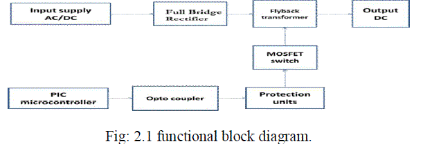 |
| A fixed input of 12V (AC or DC) is given to the system. In case of AC input, it is rectified to DC by a full bridge rectifier. So the voltage applied across the primary of the fly-back transformer is DC. A MOSFET switch is connected in series with the primary of the fly-back transformer. The voltage pulse needed to control the switch is generated by PIC microcontroller. PIC generates a pulse whose duty ratio can be varied from 0 to 50%. When the duty ratio varies from zero to fifty percent the average value of voltage induced in primary of transformer varies. So output varies from zero to 44volts. The controller circuit and power circuit is isolated using opto coupler. Various protection units were also employed to ensure proper working. The output is taken across a resistive load. |
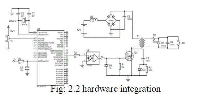
| 2.2 HARDWARE INTEGRATION |
| The complete circuit diagram is shown below in which two main parts can be seen. Left portion is the controller part in which the necessary components for controller functioning is shown. The right portion is the power circuit, where a bridge rectifier, transformer, MOSFET switch and some protection units can be seen along with output section. In between an opto coupler is provided to isolate both power part and controller part. The circuit is shown in fig 2.2 |
 |
| WORKING |
| The input can be AC or DC of 12V. An input choke filter is used to limit the high starting current, source protection and to avoid ripples in the supply. A full bridge rectifier is used to rectify the input, if it is AC. A capacitor is used to avoid ripples in rectified output. When the gate pulse is high, switch is on and the transformers to restore energy. The output diode will be reverse biased. The energy stored in output capacitor discharges to load. When gate pulse is low, switch is off and output diode is forward biased and so output capacitor stores energy and dissipates in load. Diode D2 is used to avoid negative ripples in output .Diode D1 is used to by-pass the negative ripples. |
| In controller circuit, a power on reset is given by the series combination of a resistor and capacitor, to start the operation of PIC only after the supply becomes steady. A 7805 regulator IC is used to provide 5V dc supply to the microcontroller from 12V input. A crystal oscillator of 20MHz frequency is included to drive the internal clock of the PIC. A potentiometer is used to control the duty cycle of gate pulse. For the given MOSFET switch the maximum duty cycle allowed is 60%. If the duty ratio goes beyond this value, switch will be overheated and damaged. If duty ratio become very less, then primary number of turns of transformer need to be high. This will lead to losses and reduced efficiency. For this fly-back transformer the maximum duty cycle allowed is 50%. That is if the duty cycle is greater than 50% the operation will be discontinuous and it cannot drive the load continuously. So combining all these, the maximum duty ratio is taken as 50%. When potentiometer is adjusted from minimum to maximum value, a voltage of range 0 to 5 volt is obtained. ThisanalogvalueisreadbyPICandisconvertedtodigitalvalueof10bit. The duty cycle register of PIC is of only 8 bit, so the digital data is converted to 8bit (0 to 256). If the value is greater than 128 (50%dutycycle), it is treated as 128 itself. So when potentiometer is varied from minimum to middle, a pulse of duty ratio 0 to 50% is obtained. This pulse is applied as a gate pulse to MOSFET switch. An opto coupler that can operate at 78.12 kHz is used to isolate the power circuit and control circuit. It requires 12V dc supply which needs to be isolated from the supply of PIC. It is a step up opto coupler whose input is 5V and output is 12V. Resistor R2 is used to limit the current to opto coupler. A MOSFET that can operate on the given frequency is selected. A zener diode is used to fix the voltage applied across gate and source of MOSFET as 12V. A series resistor R9 is used to limit the input current to zener diode otherwise it will burn out like any other device. Resistor R1 is used to provide the voltage signal as voltage drop across gate and source of MOSFET. Snubber circuit is used to provide a bypass path for leakage flux on primary side of transformer. |
| The turns ratio of transformer is provided such that the maximum output obtained is 44V. So when potentiometer is adjusted, a constant DC voltage of 0 to 44V is obtained for a fixed input of 12V. |
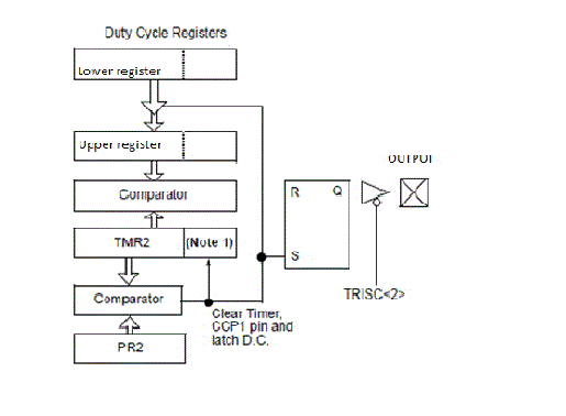
PWM GENERATION FLOWCHART |
 |
| 2.3 SOFTWARE |
| The algorithm for generating PWM pulse is represented as flowchart below |
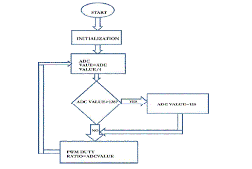 |
| The voltage drop across potentiometer is read by the PIC and is converted to 10 bit digital data (0 to 1024). Since the duty cycle register is only8 bit, the 10 bit data is converted to 8 bit (0 to 256) by dividing 10 bit data by 4. The maximum duty ratio allowed is 50% (128). So if value read is greater than 128 (50% of 256) the value is treated as 128 itself. A value less than 128 is taken as such. Thus if potentiometer is adjusted from minimum to middle position a pulse of duty ratio 0 to 50% is obtained. |
FLYBACK TRANSFORMER DESIGN |
| 2.4 Design parameters for a fly-back transformer |
| The following equations are frequently used to specify a fly-back transformer. They are followed by a typical design example. |
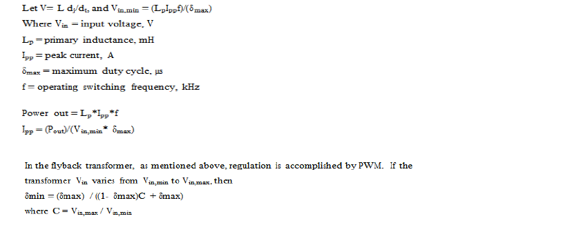 |
| The primary inductance plays an important role in the design of flyback transformer. To maintain high efficiency, the primary inductance is kept high to reduce magnetising current and lower wire losses. Thismeans the core should have aminimalair gap. |
| Since Ipp is known, Lp= (Vin,min* δmax) / (Ipp*f) |
| Next step is to select the match core. Ferrite is an ideal core material for transformers, inverters and inductors in the frequency range 20 kHz to 3 MHz, due to the combination of low core cost and low core losses. Ferrite cores also be used in fly-back transformer designs, which offer low core cost, low circuit cost and high voltage capability. |
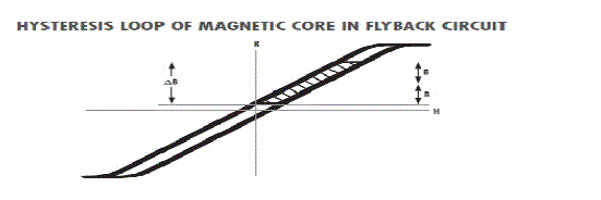
| We all know the typical transformer characteristics in terms of its B-H loop. Based on the way, how converters utilise the transformer core, they can be divided as unidirectional core excitation and bidirectional core excitation. Fly-back converter which is derived from buck-boost converter provides electrical isolation by means of unidirectional core excitation where only the positive part of B-H loop is used. |
 |
| Although designers may rely on experience for core selection, that can only result in an approximation. The following formula is recommended for a better estimate. |
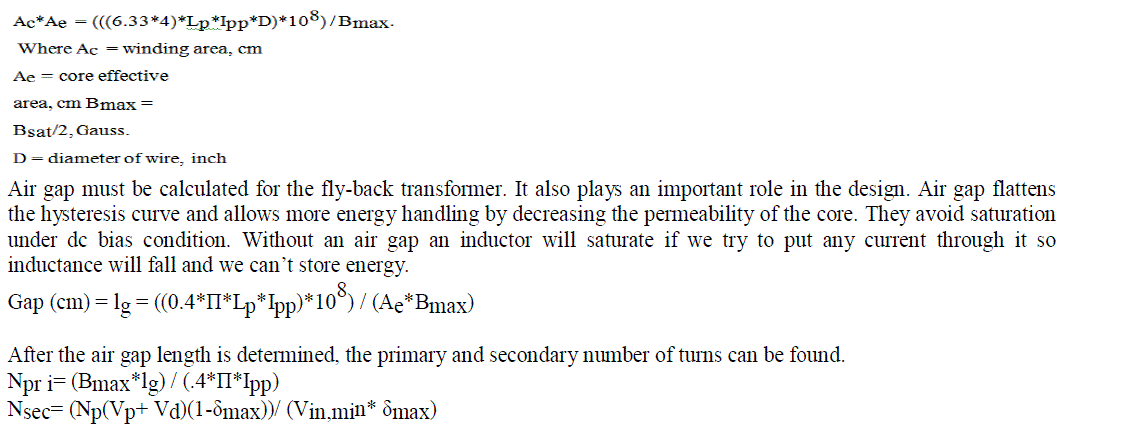 |
HARDWARE RESULTS |
2.5 OUTPUT WAVEFORMS FOR DC INPUTS |
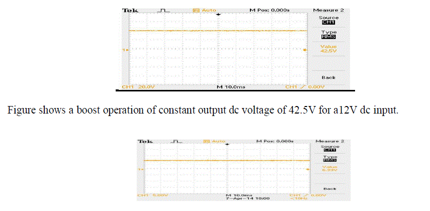 |
| Figure shows buck operation, such that for a12Vdc input, it giving 7V constant dc output. |
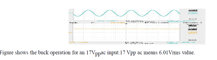
2.6 OUTPUT WAVEFORMS FOR AC INPUTS |
 |
III. CONCLUSION AND FUTURESCOPE |
| A variable DC power supply is designed using flyback principle. Here for a fixed input of 12V a variable DC output of 0 to 44V is obtained. This is a model of designing a power supply. Depending on the application and input conditions, any power supply can be designed. Flyback transformer can be designed for any required output and rectangular pulses of desired frequency and duty cycle can be generated using PIC microcontroller. |
| The future scope of this project lies in voltage regulation. As the load increases output voltage drops. So regulation can be provided to make the output constant. Microcontroller can be made to sense the output variation and regulation can be achieved automatically. It can also be designed to get a constant output when input is varied between a lower limit and upper limit. Here also microcontroller can be made to sense the input supply variation and regulate the input supply automatically. |
| The applications of this project are low-power switch-mode power supplies (cell phone charger, standby power supply in PCs), low-cost multiple-output power supplies, high voltage supply for the CRT in TVs and audio power supplies and automobile applications. |
References |
|