Keywords
|
| double edge triggering, low power, implicit clock pulse, clock branch sharing, flip-flop. |
INTRODUCTION
|
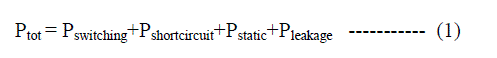
| As we know, the clock system which consists of the clock distribution network and timing elements(flip-flops and latches) is one of the most power consuming components in a VLSI system[1]. This power consumption is approximately 30% to 60% of the total power dissipation in a system. As a result of reducing power consumed by flip-flops will have a deep impact on the total power consumption. In common digital VLSI circuits,the various sources of power dissipation are switching power (Pswitching) ,short circuit power(Pshortcircuit),static power(Pstatic) and leakage power(Pleakage) [4]. The following equation describes the total power consumption(Ptot) related to these four power components. |
 |
| The important ways to reduce this power consumption are voltage scaling and double edge triggering .Voltage scaling is the most effective way to decrease power consumption, since power is proportional to the square of the voltage (the golden equation for power consumption of VLSI circuits P =CLVdd 2fclk ; where CL – load capacitance ,Vdd – supply voltage and fclk – clock frequency [7]). However, voltage scaling is associated with threshold voltage scaling which can cause the leakage to increase exponentially. On the other hand, double-edge triggered clocking can be used to save half of the power on the clock distribution network results in total power consumption. Double edge triggering means that , a flipflop responses for both positive(0 to 1 transition) and negative(1 to 0) edges results in cutting the frequency of the clock by one half . In this paper the second method-double edge triggering is proposed to implement clock branch sharing-implicit pulse(CBS_ip) scheme flip-flop and make comparison analysis with the existing double edge triggering flip-flops. |
TECHNIQUES FOR IMPLEMENTING DOUBLE EDGE TRIGGERED FLIP-FLOPS
|
| In view that, most double edge triggered flip-flops(DEFF) are developed using single edge triggered flip-flops (SEFF) design. The various SEFF are traditional master-slave FF, sense amplifier based FF, pulse triggered FF. The first two SEFF are having two stages and are characterized by a positive setup time, causing large D-Q delays. Alternatively pulse triggered FF reduces the two stages into single stage and is characterized by soft edge property. The pulsed latches have fewer clocked transistors and hence lower power consumption[3]. The pulse edge triggered flip-flops are classified in to two types : Explicit pulsed FF(ep-FF) and implicit pulsed flip-flop(ip-FF). |
| In this paper the various categories of SEFF and DEFFs are analyzed in terms of its clock pulse generating schemes as well as the data latch scheme. Generally the DEFF design will use more clocked transistors than SEFF design . However, the DEFF design should not increase the clock load too much. The DEFF design should aim at saving energy on both the clock distribution network (by halving the frequency) and flip-flops. It is preferable to reduce circuit’s clock loads by minimizing the number of clocked transistors . Furthermore, from the equation (1) ,circuits with reduced switching activity would be preferable. Low swing capability is also very helpful to further reduce the voltage on the clock distribution network for power saving. Due to the fact that voltage scaling can reduce power efficiently, the cluster voltage scaling (CVS) systems are also preferred. The various techniques to implement double edge triggered flip-flops are conventional master slave scheme ,explicit pulse triggered scheme and implicit pulse triggered scheme. In contrast, the various implicit pulse triggered schemes are symmetric pulse generator(SPGFF) scheme, conditional pre-charge(DECPFF) and the clock branch sharing-implicit pulse(CBS_ip)schemes[1]. |
REVIEW OF DETFF
|
| When the Single Edge Trigger(SET) clocking strategy is replaced by the Double Edge Trigger(DET) strategy, the performance of the DEFF must be comparable to the original SEFF(Fig.1) in order to exploit the power savings due to halved clock frequency. If the clock load of a DEFF is much larger than that of the SEFF, power savings due to the clock frequency reduction might be cancelled by an increase in the switching capacitance. Therefore, the clock load is a crucial performance parameter of a DEFF. In this section, we give the review of the state-of-the-art DEFFs and examine their characteristics that affect the performance and energy consumption. |
| A. Latch-MUX |
| 1)Transmission-Gate Latch-MUX: |
| The transmission-gate latch-MUX (TGLM) [6] is dual-edge counterpart of the single-edge transmission-gate master-slave latch (SE-TGMS)[6]. The TGLM requires two complementary clock phases. The TGLM is the straightforward implementation of the latch-MUX structure that uses transmission-gate (TG) latches. The clock load of the TGLM is large, since each Clk and CKD drives twice as many large transistors compared to the TGMS latch. Thus, even though the TGLM offers good energy-delay tradeoff, large clock load may impair the benefits obtained by operation at reduced clock frequency. |
| 2)C2MOS Latch-MUX: |
| The C2MOS latch-MUX (C2MOSLM) [6], Fig. 2 (a), is dual-edge version of the C2MOS master-slave latch . The latch used in the C2MOS LM is the conventional clocked CMOS latch. The multiplexer consists of two clocked CMOS inverters, high-Z-wired at the output, and a buffer inverter. During the time when CLK=0, the forward path of the transparent latch M1-M2, the feedback path of the opaque latch M9-M10 , and the path of the multiplexer M7- M8 are ON. Similarly, during the time when CLK=1 , the forward path of the transparent latch M11-M12 , the feedback path of the opaque latch M3-M4, and the path of the multiplexer – are ON. The C2MOSLM exploits this property of latch-MUX structure to share the clock transistors. In Fig.2(a), only one pair of clocked transistors ( M14/M15 or M13/M16 ) is used for forward path of one latch, feedback path of the other latch, and multiplexer, at the same time. This transistor sharing greatly reduces clock load and power consumption, while not compromising the performance. |
| B. Pulsed Latches |
| DE-TGPL [6], Fig.3 is DET counterpart of the single ended transmission-gate pulsed latch (TGPL) . It consists of the clock pulse generator and the TG latch. The clock pulse generator creates a short pulse after each clock edge. During each pulse, the TG latch becomes transparent and captures the input data. At all other times, the latch is opaque and the change of the output is not allowed. The pulse after each clock edge is obtained by performing the XOR/XNOR function of the input clock and the delayed clock. The delayed clock is obtained using an odd number of inverters. In this way,the clock and the delayed clock are at the same logic level only during the short time after both edges of the clock. In Fig.3, the XOR pass-transistor logic gate is used to obtain a short negative pulse at the node CP, and a short positive pulse at the node CN after each clock edge. |
| The main advantage of the DE-TGPL compared to the DET latch-MUXs is its speed[6]. An indication of the timing overhead of this pulsed latch can be obtained by observing that the D-to-Q path traverses only a single TG and an inverter. However, this timing overhead is somewhat degraded by the delay needed to generate the inverted clock pulse CN from CP, which causes an asymmetry between low-to-high and high-to-low setup and hold times. The power consumption of the DETGPL is dominated by the clock activity, due to the large switching activity of the clock pulse generator. In addition, both pass gates in the XOR gate are simultaneously open for a short time whenever the clock is switching. As a result, a contention exists at each edge of the clock that causes an increase in overall power consumption. The clock load of the DETGPL consists of the input load of an unbuffered pass-transistor XOR gate. Therefore, it is considerably larger than the clock load of the corresponding SET TGPL, which consists of one static NAND gate and one inverter[6]. |
| The other two advanced DET flip-flops described below allow clock frequency reduction while maintaining comparable timing overhead and clock load to the conventional SETSE. |
| 2)DET Conditional Precharge Flip-Flop |
| One approach for obtaining a DET flip-flop from a transparency window-based SET flip-flop is to generate a transparency window after each clock edge. The simplest way to do this is to generate an XOR logic function of the clock and the delayed clock. Another method, logically equivalent to the above, but simpler to implement, generates the signal CKD that switches low as a result of the rising edge of the delayed clock CK2, and switches high as a result of falling edge of the clock Clk. Logical AND of CKD and Clk gives the transparency window after the rising edge of the clock. Similarly, logical AND of CKD and the four-inverter-delayed clock CK4 provides the transparency window after the falling edge of the clock. Applying this method to the SET CPFF [6], we obtain the DE-CPFF, shown in Fig.4. The internal node S’ evaluates (discharges) during these transparency windows if input D=1 . Outside of the transparency windows, the path from the node S’ to ground through the transistors M1,M2,M3 is OFF, and either M7 or the series M8,M9 are ON. Thus, the node S’ takes value of D NAND Q. |
| During the transparency windows, conditional evaluation of the node S’ takes place, based on the previous level of the output Q. If Q was low in the previous clock half-cycle, the node S’ was precharged high. In the transparency window, the node S’ switches low if D is high (either the path M1-M3 – M4 or the path M2-M3 –M4 is on). As a result, Q switches high via transistor M16. If the input D is low, the node S’ remains high and Q remains low. If Q was high in the previous clock half-cycle, the node S’ took value of the inverted input D (M4,M5 andM6). When a transparency window arrives, the high level of S’ causes Q to switch low (paths M11-M13 –M14 and M12-M13 –M14 ). The low level of S’ has no effect to Q, as it was already high. Once the node S’ is low, it can return to the high level only if the input is low. In other words, the node S’ does not exercise pre-charge-evaluate sequence in each clock cycle. Therefore, internal power consumed for the redundant pre-charge for the case D=Q=1 is saved. Consequently, this flip-flop has the feature of conditional precharge and statistically reduces power consumption for low input activity. |
DOUBLE EDGE CLOCK BRANCH SHARING IMPLICIT PULSED FLIP-FLOPS(CBS_IP)
|
| The conventional DEFFs duplicate the area and the load on the inputs[1]. Explicit pulsed DEFFs use external clock pulse generators, which increase the power. In addition, explicit pulsed DEFFs cannot work with dynamic logic. SPGFF uses implicit pulsing; however, it has four internal redundant switching nodes. Unlike SPGFF, DECPFF eliminates the redundant switching activity, however, the number of clocked transistors reaches 21, and the clock branch duplicating structure is complex. |
| To ensure efficient implementation of double-edge clock triggering in an implicit pulsed environment and to overcome the problem with previous implicit pulsed flip-flops which is the large clock load, a novel clock branch sharing topology is used. The sharing concept is similar to the single transistor clocked FF and another clock branch sharing flip-flop. The advantage of this sharing concept is reflected in reducing the number of transistors required to implement the clocking branch of the double-edge triggered implicit-pulsed flip-flops. Without this sharing, the number of clocked transistors would be much larger than the number of transistors used with the sharing concept. Recall that clocked transistors consume a large amount of power. Reducing the number of clocked transistors is an efficient way to decrease the power . The CBS_ip uses the pseudo nMOS logic resulting from the conditional discharge technique. |
SETFF AND DETFF SIMULATION RESULTS AND PERFORMANCE COMPARISON
|
| The simulation results are obtained from PSPICE simulation tool (version 9.2) for 0.18um CMOS technology[2] at room temperature. Each design is simulated using the circuit at the schematic level in PSPICE AD and results are verified through transient analysis. |
| In this paper, First the simulation results are obtained for the designs of SEFF[Fig.1(b)],C2MOS latch- MUX[Fig.2(b)], DE-CPFF[Fig.5], CBS_ip DEFF[Fig.6(b)] and power consumption for the said designs are extracted from their corresponding output files and are shown in table 1. From table 1 , the comparisons are made in terms of number of transistors ,clock frequency and power consumption .It is illustrated in the graph Fig.8. Second it is designed 2 bit Serial- In-Serial-Out(SISO) shift registers for the designs C2MOS latch-MUX[fig.2(c) and CBS_ip DEFF[Fig.7] and their outputs are verified. The performance are compared in terms of number of transistors and power consumption and is listed in table 2. It is inferred from the results that,the power consumption is less for CBS_ip DEFF design as compared to C2MOS latch- MUX design is illustrated in the fig.9. |
CONCLUSION
|
| In this paper, it is survived to implement low-power shift register using a double edge triggered flip-flop and make comparison analysis between various existing design. The flip-flops(FF) in the proposed shift register are designed using clock branch-sharing. The various existing double edge triggered flip-flops are transmission-gate latch-MUX, C2MOS Latch-MUX, Dual-edge transmission-gate pulsed latch (DE-TGPL),CPDEFF and CBS_ip DEFF. From the simulation results shown in table 2 it is inferred that the proposed shift register designed using CBS_ip has an improvement in power consumption as compared to the other state of the art double-edge triggered flip-flop designs. Since the proposed design has less number of clocked transistors and lowest power, it is suitable for high-performance and low power environments. |
Tables at a glance
|
 |
| Table 1 |
|
Figures at a glance
|
 |
 |
 |
 |
 |
| Figure 1a |
Figure 1b |
Figure 2a |
Figure 2b |
Figure 2c |
|
 |
 |
 |
 |
| Figure 3 |
Figure 4 |
Figure 5 |
Figure 6a |
|
 |
 |
 |
 |
| Figure 6b |
Figure 7 |
Figure 8 |
Figure 9 |
|
References
|
- Peiyi Zhao, Jason McNeely, Pradeep Golconda, Magdy A. Bayoumi, Robert A. Barcenas, and WeidongKuang ,” Low-Power Clock Branch Sharing Double-Edge Triggered Flip-Flop”, IEEE transactions Very Large Scale Integration (VLSI) Systems, Vol. 15, No. 3, 338-345,March 2007.
- David A. Hodges, Horace G. Jackson, ResveSaleh, Resve A. Saleh, “Analysis and design of digital integrated circuits: in deep submicron technology” Mc.Graw-Hill, 2nd Edition,2003.
- Weste N and Harris D, “CMOS VLSI Design”. 3rd edition, Addison Wesley, 2007.
- Kim C C and Kang S, “A low-swing clock double edge-triggered flip-flop,” IEEE J. Solid-State Circuits, vol. 37, no. 5, pp. 648–652, May2002.
- Chung W and Sachdev M, “A comparative analysis of low power low-voltage dual-edge-triggered flip-flops,” .IEEE Trans. Very Large ScaleIntegr. (VLSI) Syst., vol. 10, no. 6, pp. 913–918, Dec. 2002.
- Nikola Nedovic and Vojin G.Oklobdzija,”Dual-edge triggered storage elements and clocking strategy for low -power systems”,IEEE transactions on VLSI systems, Vol.13,No.5, pp. 577-590,May2005.
|