Keywords
|
| Microstrip Patch Antenna, Parasitic Elements, HFSS, Coaxial Probe |
I.INTRODUCTION
|
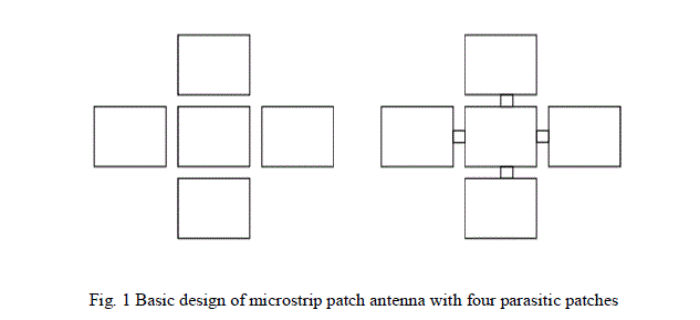
| This method is chosen to investigate how the Parasitic Patch configuration [1-4] can improve the bandwidth of a typical microstrip antenna. In this type of antenna design, patches are placed near the edges of the original patch. These new patches may be coupled to the main patch electro-magnetically or through the direct coupling technique. Each patch can be designed in a similar manner to the original patch. The lengths of the parasitic patches will determine their resonant frequency and their width will determine the bandwidth they display at resonance. In this project we also use four parasitic patches to enhance the bandwidth of antenna. Two patches are along radiating side and other two are along non-radiating side. Dimension of both sides of parasitic patches is same. Active patch has greater length and width than other four patches. Patch along non-radiating side has smaller dimension than others. Basic design of antenna with parasitic elements is shown in Fig. 1. |
 |
| Broadband Gap-Coupled Slot Cut Rectangular Microstrip Antennas: A Review |
| The broadband microstrip antenna (MSA) is realized by fabricating the patch on lower dielectric constant thicker substrate. However for substrate thickness (h) more than 0.04λ0, the bandwidth (BW) is limited by the feed probe inductance. For h > 0.06λ0, the BW is increased by using proximity feeding technique. The BW is also increased by using multi-resonator gap-coupled configurations. However this method increases the antenna size. More commonly the antenna BW is increased by cutting the slots of shapes like, U-slot, V-slot, and rectangular slot at an appropriate position inside the patch. The slot is said to introduce a mode near the fundamental mode of the patch and yields larger BW. In most of the reported designs the slot length is either taken equal to half wave or quarter wave in length at the desired slot frequency. The gain of the antenna is increased by using the gap-coupled configurations or by using the arrays of the individual patch elements. The broadband E-shaped MSA is realized by cutting the pair of rectangular slots on one of the radiating edges of the patch. |
| In the reported design the slot length is assumed to be nearly quarter wave in length. In this paper, broadband proximity fed E-shaped MSA is discussed. The E-shaped MSA gives a bandwidth of nearly 350 MHz with broadside radiation pattern with gain of more than 7 dBi over the VSWR BW. Further a gap-coupled configuration of parasitic rectangular MSAs (RMSA) with an E-shaped MSA is proposed. This configuration gives a BW of more than 450MHz at center frequency of around 1000 MHz. The proposed antenna gives broadside radiation pattern with peak gain of nearly 9 dBi. Further increase in the BW of above gap-coupled configuration is realized by cutting the pair of rectangular slots along the non-radiating edges of the gap-coupled RMSAs. This configuration gives a BW of more than 550 MHz at center frequency of 1000 MHz. The radiation pattern is in the broadside direction with peak gain of more than 9 dBi. All these configurations have been first analyzed using IE3D software followed by experimental verifications. The dimensions of the individual patches were optimized such that they cover 800 – 1200 MHz frequency band. The air substrate is used to maximize the radiation efficiency and gain. In the measurements the antennas were fabricated using copper plate and were suspended in air using the foam spacer support placed towards the antenna corners. The antenna is fed using Ntype connector of 0.32 cm inner wire diameter. The measurement was carried out using R & S vector network analyzer. Since an infinite ground plane is used in the measurements, a larger square ground plane of side length 80 cm (2.67λ0) is used in the measurements. The radiation pattern was measured in minimum reflection surrounding with the required minimum far field distance between the reference antenna and the antenna under test. The antenna gain was measured using three antenna method. |
 |
II.ANTENNA DESIGN
|
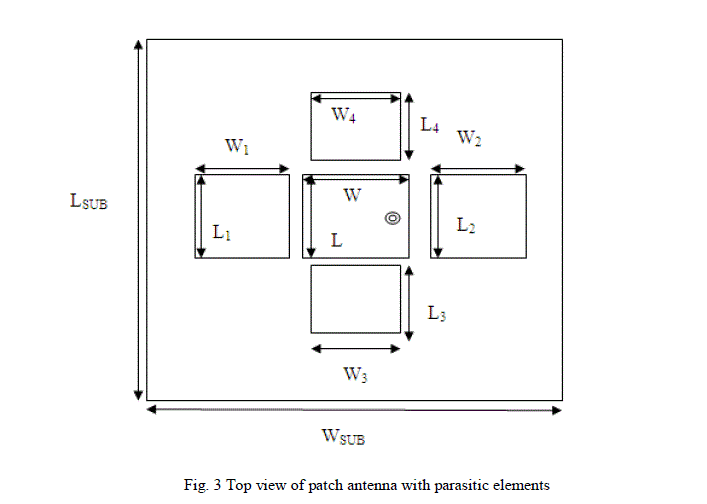
| In step 1, a simple rectangular patch antenna has been designed to resonate at 5.43 GHz by using the standard equations [5]. In step 2, two rectangular shaped patches along radiating sides of patch are designed as a result bandwidth is increased. In step 3, another two rectangular shaped patches are designed along non-radiating sides of the patch. Impedance bandwidth is increased up to 1.04 GHz. Coaxial probe feed technique is used. Top view of antenna has been shown in Fig. 2. |
 |
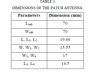
| Table 1 shows the optimized parameters of the patch and the antenna. |
 |
III. . SIMULATED RESULTS OF THE OPTIMIZED ANTENNA
|
| In this section, simulated results of the optimized antenna have been presented |
| Return Loss Plot |
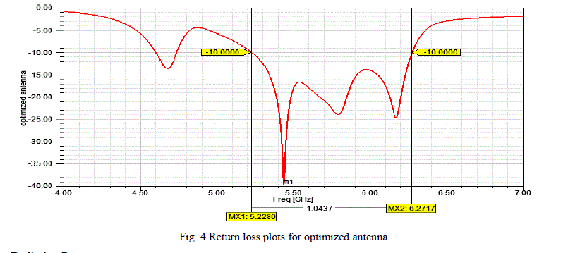
| Fig 3 shows the S11 parameters (Return loss) of the optimized E-shaped patch antenna. The return loss is considered below -10 dB. As shown in Fig. 3 the proposed antenna has been resonant on 5.43 GHz having the return loss of -39.7 dB. The bandwidth of the antenna is a range of frequencies over which the return loss is greater than -10 dB. Thus from the Fig. 5.7 the return loss below -10 dB is started from 5.22 to 6.27 GHz, the bandwidth of the optimized antenna is around 1.0437 GHz. |
 |
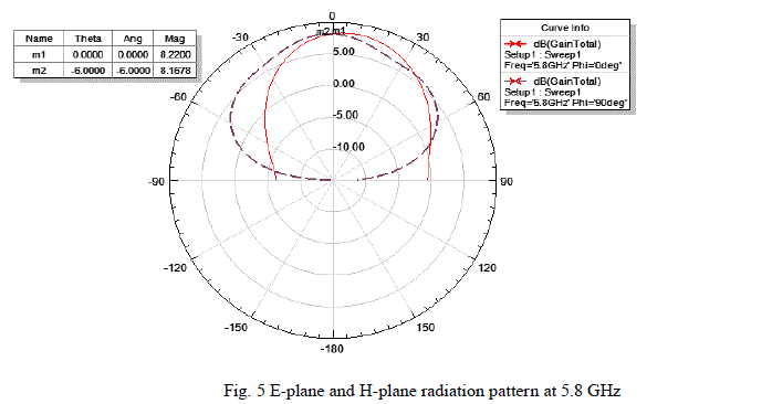
| Radiation Patterns |
| Radiation Pattern represents the power distribution of antenna radiation. It can be in omnidirectional which means it spreads the power in all directions. The radiation pattern can be shown in Fig. 4 at 5.80 GHz frequency. It is omnidirectional in shape. The maximum gain of 8.22 dB has been obtained. |
 |
IV.CONCLUSION
|
| A simple patch antenna with parasitic elements fed by coaxial probe feed has been presented. The RT/duroid 5880 material has been used as the substrate of the antenna. Four parasitic elements are used to enhance the bandwidth. The proposed antenna is resonating from 5.22 GHz to 6.27 GHz resulting in bandwidth of nearly 1.04 GHz. The maximum gain of the proposed antenna is around 9.31 dB. The proposed antenna is useful for higher speed wireless devices. HFSS software [6] is used to simulate the antenna. |
References
|
- Alipio BC, David FC, Isabel RS, Juan CNM. Manuel AE. Comparison of batch, stirred flow chamber, and column experiments to study adsorption, Desorption and transport of carbofuran within two acidic soils. Chemosphere. 2012; 88(1): 106-120.
- Arnaud B, Richard C, Michel S. A comparison of five pesticides adsorption and Desorption processes in thirteen contrasting field soils. Chemosphere. 2005; 61(5): 668-676.
- Chunxian W, Jin-Jun W, Su-Zhi Z, Zhong-Ming Z. Adsorption and Desorption of Methiopyrsulfuron in Soils. Pedosphere. 2011; 21(3): 380-388.
- Chunxian W, Suzhi Z, Guo N, Zhongming Z, Jinjun W. Adsorption and Desorption of herbicide monosulfuron-ester in Chinese soils. J Environ Sci. 2011; 23(9): 1524-1532.
- Christine MFB, Josette MF. Adsorption-desorption and leaching of phenylurea herbicides on soils. Talanta. 1996; 43(10): 1793-1802.
|