International Journal of Advanced Research in Electrical, Electronics and Instrumentation Engineering
ISSN ONLINE(2278-8875) PRINT (2320-3765)
ISSN ONLINE(2278-8875) PRINT (2320-3765)
Sonika Choubey1, Rajesh Kumar Paul2
|
| Related article at Pubmed, Scholar Google |
Visit for more related articles at International Journal of Advanced Research in Electrical, Electronics and Instrumentation Engineering
This paper deals with design of controlled adder /subtractor cell using Shannon based full adder with pass transistor logic. The proposed adder used only 14 transistors for full adder implementation. Simulations were performed by Microwind 3.1 and DSCH 2 VLSI CAD tools and BSIM 4 for parametric analysis of various features. The analysis is done on the basis of power consumption, delay and area occupied and theses are compared with previous papers and we are good to enhance these parameters.
Keywords |
| CAS, Shannon Theorem, Shannon Adder, BSIM4 |
I. INTRODUCTION |
| In recent years, most of the VLSI applications, such as DSP and microprocessors use arithmetic operation like addition and subtraction.[1] .Many multiplier (or) divider circuits have been proposed that offer lower propagation delay, low power dissipation that can be implemented by using adder and subtractor. The high speed and reduced area size can be implemented with different logic style in VLSI design [3]. There are many types of logic designs, each has its own pros and cons in terms of speed, chip size (area) and power dissipation [4]. This trend must be ceased to obviate extortionate packaging and thermal management cost at system level. Eventually as more switching is done in a particular period of time; it would cause the circuit to perform much more gradual. However this quandary can be lowered if not solved by reducing the number of transistor that is being utilized. Many transistors in a circuit might be redundant and abstracting this redundancy can avail to lower the delay and hence incrementing the speed. This CAS cell is designed utilizing accumulation of full adder and 2 input XOR. The Shannon theorem predicated adder circuit can be reduced the number of transistor utilizing by redundancy reduction method. |
| The Shannon theorem adder circuit used only the NMOS, which would decrement the internal capacitance and reduce the propagation delay. The divider circuit parameters analysed utilizing by BSIM4 analyser. We have compared our results with three other adder cell predicated divider circuits in terms of speed, area and power dissipation. |
II. FULL ADDER |
| A Full Adder is a basic cell component of the digital systems. It has three inputs and two outputs, sum and carry. It performs the addition of the three inputs and produces the sum and carry. The standard Boolean expressions are given as: |
| SUM = ABC+A’BC’+A’B’C+AB’C’ (1) |
| CARRY = AB+BC+CA (2) |
III. SHANNON BASED FULL ADDER |
| According to this theorem any logic expression is divided into two terms. First with a particular variable set to 1 and multiplying it by a variable and then set the variable to 0 and multiplying it by the inverse. The fullest reduction can be obtained by continuously repeating the Shannon theorem. |
| This method is useful especially to multiplier and pass transistor circuit design. The Shannon’s theorem in a generalized way can be stated as a function of many variables, f (b0, b1, b2, y, bi, y, bn) can be written as the sum of two terms, say one with a particular variable ai , set to 0, and one with it set to 1. |
| f (b0, b1, b2, ......, bi,.....y, bn) = bi’f (b0, b1, b2, ......, 0,.....y, bn) + bi f (b0, b1, b2, ......, 1,.....y, bn) (3) |
| using Shannon expansion theorem we get modified full adder equation , |
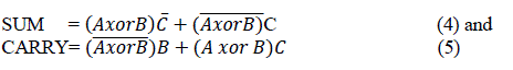 |
| By using expressions (2) and (3), the pass transistor functions can be implemented as shown in Fig.1 ,this shows the Shannon based full adder design using pass transistor logic. [5] |
 |
IV.PROPOSED ADDER/SUBTRACTOR CELL |
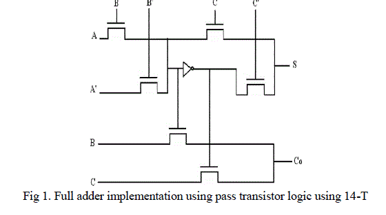
| In digital circuits, an adder–subtractor is a circuit that is capable of integrating or subtracting numbers (in particular, binary). Below is a circuit fig 2 that does integrating or subtracting depending on a control signal. It is additionally possible to construct a circuit that performs both integration and subtraction concurrently. |
 |
| that has control input D and the initial carry connect is also connected to D then: |
| When D=0 the modified adder performs addition |
| When D=1 the modified adder performs subtraction |
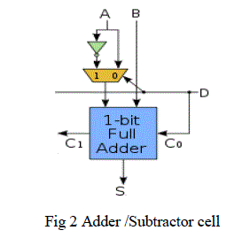
| Having a 1-bit adder for A and B, then S=A+B. Then to perform A-B, two's complement theory says to invert each bit with a NOT gate and add 1, This yields S=A+B’+1, which is easy to do with a slightly modified adder. CAS cell can be designed by using full adder and XOR gate. Because we know that the XOR gate can complement any input if other input is set to be 1. So here Fig 3 shows the schematic design of CAS cell that is implementation by DSCH 2 VLSI CAD tool. |
 |
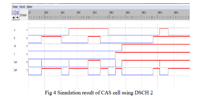
| In Fig 3 A and B, are one bit numbers used for addition / subtraction and cin is carry bit and T is test bit that is responsible for the behaviour of controlled adder/subtractor as a adder or subtractor .Sum/Difference and Carry/Borrow are output variables shown by LED outputs sum and carry . For verifying architectural behaviour simulation result is required so Fig 4 showing the simulation result done by using DSCH 2 tool for schematic design shown in Fig 3. |
 |
V. RESULT AND DISCUSSION |
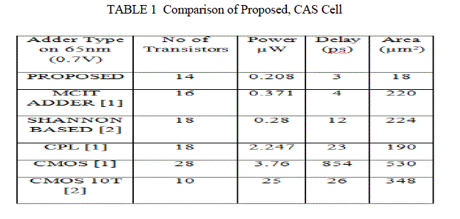
| The purpose of this designing task is to make a comparison on which adder will give us a good performance, once it is implemented into the cells. Our proposed Shannon adder is designed by using 65nm corresponding supply voltages are 0.7V For the analysis of various parameters such as area, propagation delay, dissipated power, BSIM4 is used and our design is efficient than previously design adder. Table 1 showing that our design is more efficient then other in terms of all parameters. |
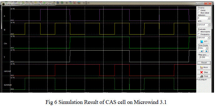
| For designing and simulation of our circuit at physical description level here Microwind 3.1 software is going to use. Fig 5 showing the layout design of proposed CAS cell and fig 6 giving the simulation result for the layout .Fig 4 and 6 are verifying our design as a adder /subtractor cell . |
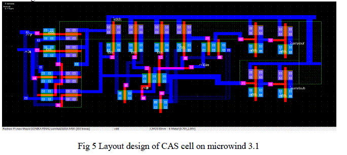 |
| Here 65nm technology is used for implementing the design so corresponding supply voltage for above design is 0.7V and all parameter analysis is done by BSIM4 analyser that is inbuilt in Microwind 3.1 software. |
 |
 |
VI.CONCLUSION |
| An adder circuit is designed by utilizing Shannon theorem and implemented into the design of adder/subtractor circuit. The proposed adder/subtractor circuit gives more preponderant performance. It compared its delay and area efficiency. Furthermore, this adder/subtractor cell can be use in divider, due to the utilization of Shannon predicated adder design approach . The proposed adder/subtractor circuit circuit may utilized in DSP circuits, divider and multipliers due to low power dissipation, less propagation delay and lower area. |
References |
|