International Journal of Advanced Research in Electrical, Electronics and Instrumentation Engineering
ISSN ONLINE(2278-8875) PRINT (2320-3765)
ISSN ONLINE(2278-8875) PRINT (2320-3765)
Swapnil Zadey1, Subroto Dutt2
|
| Related article at Pubmed, Scholar Google |
Visit for more related articles at International Journal of Advanced Research in Electrical, Electronics and Instrumentation Engineering
The solar energy conversion system is an alternative for conventional power generating system. It has no running cost due to freely available and non polluting solar radiations. The voltage which is available from solar array is variable and to obtain a stable voltage from solar panels, DC-DC converters are required for constant power production. There are mainly three converters namely Buck, Boost and Buck-Boost converters which can be used for either increasing or decreasing the voltage. This paper presents mobile charging circuit with a PV source. The circuit structure of the proposed system adopts buck converter combined PWM MPPT technique. In this research, buck converter is used as a charger for charging mobile battery. The input voltage can typically change from (12V) initially, down to (5V), and provide a regulated voltage within the range of the 4.5V required for the charging of mobile batteries.
Keywords |
| Buck converter, MOSFET, Mobile charging system, MPPT technique,PV system. |
I. INTRODUCTION |
| DC-DC converters are considered to be of great economical importance in today’s society, and are perhaps one of the few electronic circuits that are commonly used in switching power supplies, generally are widely used at home solar systems to produce the desired output power[6]. More sophisticated applications require electronic converters to process the electricity from the PV device. These converters may be used to regulate the voltage and current at the load, control the power flow in grid-connected systems, and mainly track the maximum power point (MPP) of the device[10]. Therefore, this paper tries to study an electronic converter in PV systems, namely the Buck converter, and propose an easy way to electronic converter designers to calculate component values needed to realize it. |
| A. DC-DC Converters |
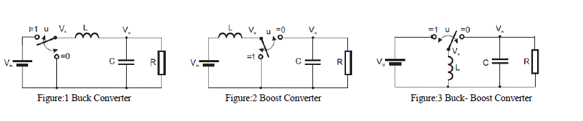
| There are three kinds of switching mode DC-DC converters, buck, boost and buck-boost. The buck mode is used to reduce output voltage, whilst the boost mode can increase the output voltage. In the buck-boost mode, the output voltage can be maintained either higher or lower than the source but in the opposite polarity. The simplest forms of these converters are schematically represented in Figure 1,2& 3. These converters consist of the same components, an inductor, L, a capacitor, C and a switch, which has two states u = 1 and u = 0. All converters connect to a DC power source with a voltage (unregulated), Vin and provide a regulated voltage, vo to the load resistor, R by controlling the state of the switch. In some situations, the load also could be inductive, for example a DC motor, or approximately, a current load, for example in a cascade configuration. For simplicity, here, only current and resistive loads are to be considered. |
 |
| B. Working Principles: |
| The working principles of the DC-DC converters can be explained as follows. In the buck mode, when the switch is on position 1, the DC source supplies power to the circuit which results an output voltage across the resistor. When the switch changes its position to 0, the energy stored in the inductor and capacitor will discharge through the resistor. Appropriately controlling the switching position can maintain the output voltage at a desired level lower than the source. |
| In the boost mode, when the switch is on position 1, the circuit is separated into two parts: on the left, the source is charging the inductor, meanwhile the capacitor on the right maintains the output voltage using previously stored energy. When the switch changes its position to 0, both the DC source and energy stored in the inductor will supply power to the circuit on the right, hence boost the output voltage. Again, the output voltage can be maintained at desired level by controlling the switching sequence. |
| Finally, for the buck-boost mode, switch positions 1 and 0 represents charging and discharging modes of the inductor. Appropriately controlling the switching sequence can result in output voltage higher or lower than the DC source. Since the inductor cannot change the direction of current, the output voltage is opposite to the DC source. This paper provides the designing and simulation of Buck converter. The reason to choose a Buck converter is that our load is a 4.5V mobile battery, where we will charge it with only one PV module which generates the most watts running at around 12 V. Thus, we need a DC/DC converter which takes a higher input voltage and converts it to a lower output voltage. This can only be done by the Buck converter. We will, first, start by a brief introduction to the functioning of a Buck converter, and then, write its basic equations. |
II. WORKING OF BUCK CONVERTER IN BRIEF |
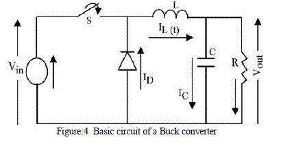
| I. Circuit description: |
| The basic circuit of a Buck converter is shown below in Figure 4. Two switches are used in this basic circuit, usually one controlled (MOSFET) and one uncontrolled (diode), to achieve unidirectional power flow from the input to theoutput. This circuit, also, uses one capacitor and one inductor to store and transfer energy from input to output. They, also, filter or smooth voltage and current[10]. |
 |
| II. Circuit operation: |
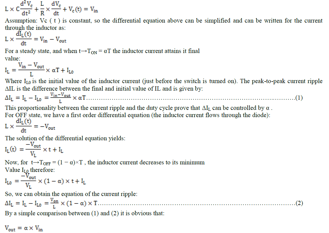
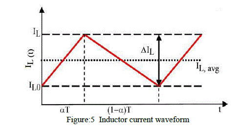
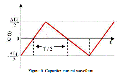
| We used inductors and capacitors as energy storage components to control the energy flow from the input to the output by continuously opening and closing the switch which is usually an electronic device that operates in two states: When the switch is ON for a time duration αT ( α is the duty cycle), the switch conducts the inductor current and the diode becomes reverse biased. This results in a positive voltage VL = Vin − Vout across the inductor. This voltage causes a linear increase in the inductor current IL . When the switch is turned OFF , because of the inductive energy storage, IL continues to flow. This current now flows through the diode, and VL = − Vout for a time duration (1 − α)T until the switch is turned ON again. The basic circuit of the Buck converter showed in Figure 1 has two energy storage elements: the inductor and capacitor which can be calculated in a second order differential equation. We start by the differential equation for the capacitor voltage, in the ON state, which given by: |
 |
 |
 |
 |
 |
 |
IV.SIMULINK MODEL |
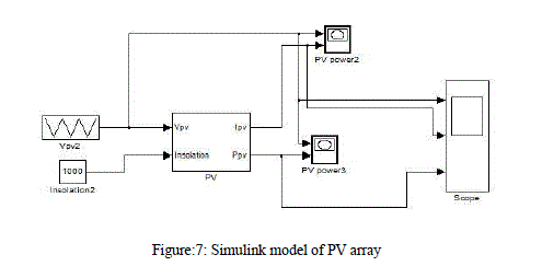
| Simulink Model of PV array is shown in figure below which is then simulated to obtain result by using variable input radiation parameters: |
 |
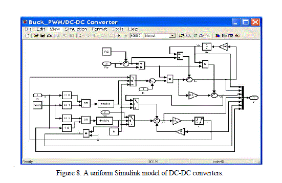
| These three modes of DC-DC converters have been uniformly implemented in the MATLAB/Simulink as show in Figure 8. |
 |
| The input-output connections of the model is shown in Figure 9. The first input to the model is the switch |
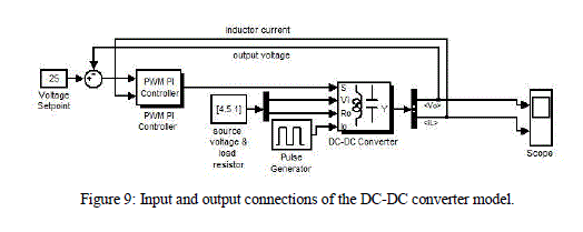 |
| signal eight 1 or 0. The second one defines the DC source voltage and internal resistance. The third input is used to define the output current. The model has two outputs, the output voltage and the inductor current, which are the states of the system. The model can be configure with a number of parameters. These parameters are: the capacitance, C, inductance, L, the internal resistance of the capacitor and the inductor, RC and RL respectively. Three converter modes can be selected through the pull-down menu. One can also define either zero or non-zero value to the initial capacitor voltage by selecting or de selecting the “zero capacitor voltage" option. Finally, the option “Positive Inductor Current" defines whether the condition should be enforced or not. |
III. SIMULATION RESULTS |
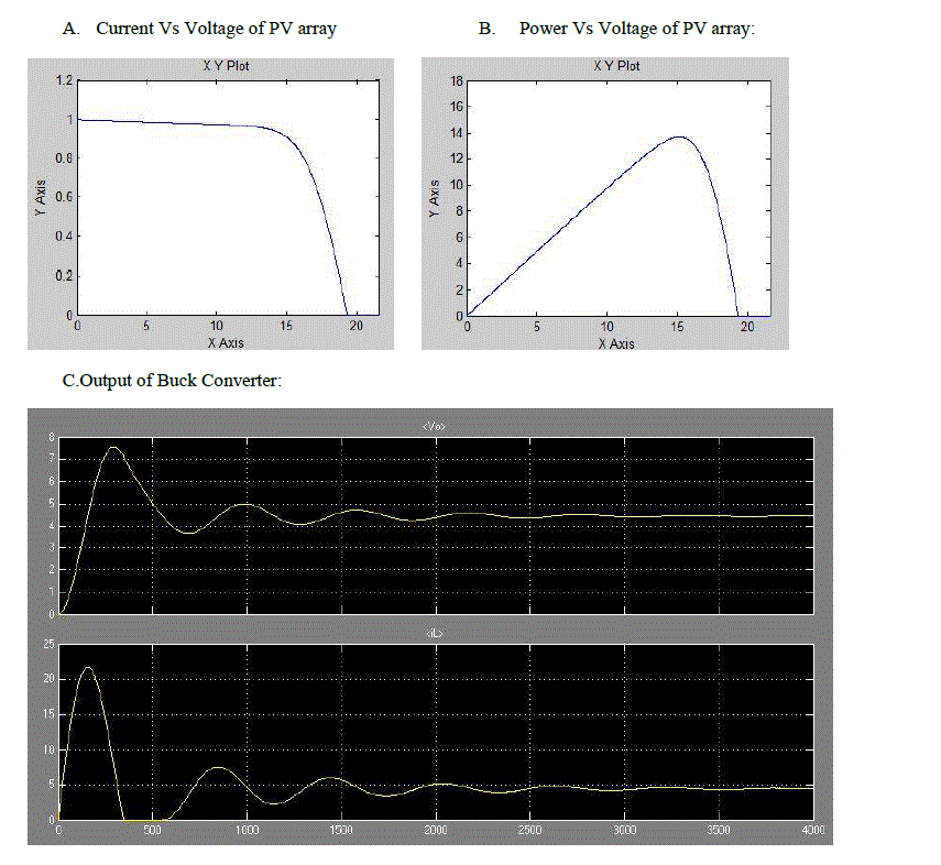
| After simulating the above equations and above models, following results can be obtained: |
 |
IV. CONCLUSION |
| Thus in this paper, a buck converter is designed and simulated successfully to obtain the constant output of about4.5V integrated with mobile charging circuit to charge the mobile. From simulation results, it can be seen that by using buck converter, we were able to convert variable voltage and current into a constant one. As the solar panel provides variable current and voltage depending upon the solar radiations, we used PWM MPPT technique to obtain continuous maximum power output which is then given input to the buck converter. Our further research work will be in comparative study of converters namely Buck, Boost and Cuk converter. |
References |
|