Keywords
|
| Asynchronous Data Sampling, Double Edge Triggered Flip-Flop, Clock Gating |
INTRODUCTION
|
| Power consumption is becoming an crucial factor in digital designs. For a digital system, the power spent on the clock-tree and the storage element is a major source of power consumption. The Clock system accounts for 30% to 60% of the total power dissipation. As a result, deducing the power consumed by storage elements such as flip-flops and clock system will have a deep impact on the total power consumption. One effective and efficient approach is Double edge triggered flip flop (DETFF).Dual edge clocking requires Dual Edge-Triggered Storage Elements (DETSE), capable of capturing data on both rising and falling edge of the clock. Main advantage of DETSE is their operation at half the frequency of the conventional single-edge clocking, while obtaining the same data throughput. The second technique is Clock-gating for a large digital system, clock-gating technique is used to reduce the power consumed on idle circuitry in the design. The DETFF and clock gating combined together to further reduce dynamic power but it introduces the asynchronous data sampling problem between the clock edges at the output side it creates the data miss-communication error. This paper deals with the design of shift register with DETFF various clock gated DETFF proposed to analyze the sampling problem |
EXISTING SYSTEM
|
| A. Double Edge Triggered Half-Static Clock-Gated D Flip-Flop: |
| The Double Edge triggered half Static Clock Gated D-type Flip-Flop (DHSCGFF) design[1] ,which consists of two identical dynamic master latches and a half-static slave latch. Compared with the SET implementation[2], this DHSCGFF consists of an additional master latch in parallel to the original master latch. Unlike Yu's circuit[3], the proposed circuit does not swap the use of master and slave latches in alternative clock phases to avoid the problem of coupling the half-static latch directly to the input data path. Instead, these two master latches are triggered in alternative clock edges, which are controlled by two complementary signals C and Cbar.. |
| A half-static slave latch stores the data from each master latch in alternative clock phases. The clock-gating circuit compares D with Q and outputs a logic "HIGH" at R to turn transistor M2 off when D = Q. This configuration suppresses the control signal C by deactivating the inverter chain. The core of the flip-flop is edge-triggered by C and Cbar so that it does not require the use of any pulse generator to generate a pulse-like transparent window within the flip-flop. The pass transistor logic simplifies the circuit and reduces the internal power dissipation.The circuit complexity and transistor count of the DHSCGFF is reduced by using pass transistor based clock-gating circuit, dynamic master latches and half-static slave latch, and thus reduces the total power dissipation. In contrast to other Latch-Mux double edge-triggered flip-flops that place a logic keeper at Node X2 to floating nodes (as well as the corresponding Node X1 in upper path), Tam’s design added switches MB1 and MB2 into the latch that intentionally isolate Nodes X1 and X2. |
| For transitions on D input that occur during global clock CLK=0, an asynchronous pulse is generated on internal clock. Then before switch MA2 turns OFF, there is only a very short amount of time for Node X0 to charge or discharge. If the value of X0 is strong enough to flip the nodes to the output, then an asynchronous transition will appear at the output. Otherwise, if the first trigger of the lower path has not successfully passed the input D to the output, then the upper path serves as a backup that will be triggered at the next falling edge of internal clock C. |
| C. Methodologies To Remove Asynchronous Data Sampling: |
| By adjusting the transistor sizes around Node X2 , there are multiple sets of transistor sizing that can cause the asynchronous data sampling to fully appear (i.e., show both cases), partially appear (i.e., only one case is observed) or be hidden. The condition that makes the asynchronous transition appear depen upon whether the voltage of Node X3 reaches the critical value to flip the output. |
| The circuit’s parameters such as transistor size are modified to eliminate Asynchronous Data Sampling. |
| 1. Balanced sized—the circuit produces similar rise and fall time, but one asynchronous transition appears in result. |
| 2. Modified I—this circuit demonstrates that both possible asynchronous transitions can appear. |
| 3. Modified II—the circuit demonstrates that both possible asynchronous transitions are removed. |
PROPOSED SYSTEM
|
| In the proposed system, Double Edge Triggered Flip-Flops (DETFFs)are used to built shift register in order to reduce the power consumption, as that they can able to maintain the same throughput as single edge-triggered between flip-flops (SETFFs) while only using half of the clock frequency. Clock gating is also employed in this shift register to further reduce the power consumption. Incorporating Clock gating in shift register introduces Asynchronous Data Sampling problem that produces error in output. |
| A.Shift Registers |
| In digital circuits, Shift registers are a type of sequential logic circuit, used for the storage of digital data. Shift register is a cascade of flip flops, sharing the same clock, in which the output of each flip-flop is connected to the data input of the next flip-flop in the chain, resulting in a circuit that shifts by one position the bit array stored in it, shifting in the data present at its input and shifting out the last bit in the array, at each transition of the clock input |
| The implementation of Shift register with Double Edge Triggered Flip Flop is shown in the Fig.3. The DETFF used in this design is Double Edge Triggered Half Static Clock Gated D-type Flip-Flop(DHSCGFF). The DHSCGFF is choosen for the implementation, as it consumes less power and delay and the Asynchronous Data Sampling is removed for this Flip-Flop. The data string is given a data input and is shifted right one stage each time 'Data Advance' is brought high. At each advance, the bit on the far left “Data Input” is shifted into the first flip-flop's output. The bit on the far right “Data output” is shifted out and lost. The data are stored after each flip-flop produces data output. |
| A. Scheme To Avoid Asynchronous Data Sampling |
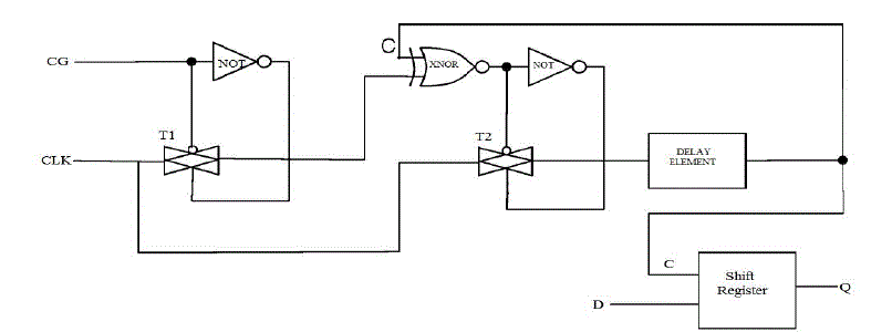
| In the Scheme shown in the Fig.4 the CLK is controlled by the comparison of D and Q. If D has changed since the last clock transition and is different from Q, then CLK will pass to the second comparator to compare with the C. This CLK and C comparator controls the switch T2 between the CLK and C. |
| This second comparator prevents the asynchronous sampling occurred in this implementation. Asynchronous sampling occurs when D changes at the moment that CLK differs from C. However, with the second CLK & C comparator in Fig.4, the switch T2 will stay OFF when CLK ≠ C and C will synchronize with CLK. In the next half cycle, the switch T2 turns ON, where CLK = C, but since they are equal, the flip-flop will not be triggered until C changes, which follows CLK when is ON. |
POWER ANALYSIS
|
| From the Table.1 it is shown that power consumption of Modified-II circuit is less when compared with DHSCGFF, Balanced size and Modified-I circuit. Modified-II circuit consumes less power because its critical parameters such as transistor’s size is modified according to circuits specified limits. |
| Thus from the Table.2, it is proven that Shift Register built with Double Edge Triggered Flip-Flop consumes less amount of average power and minimum power when compared with Shift Register built with D Flip Flop. |
| The Shift Register built with Double Edge Triggered Flip-Flop consumes less power as that it can able to produce the same throughput with half of clock frequency of Single Edge Triggered Flip-Flop and it can produce double the throughput when compared with Single Edge Triggered Flip-Flop. As the power consumption in Flip-Flop circuits greatly depends on clock frequency, reducing the clock frequency in Double Edge Triggered Flip-Flop produces a good impact in power consumption of Shift Register built with Double Edge Triggered Flip-Flop. |
RESULTS AND DISCUSSION
|
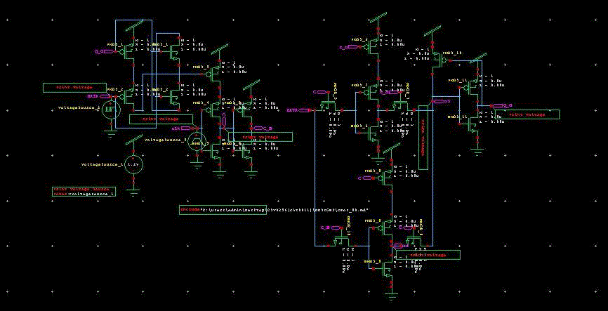
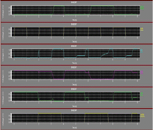
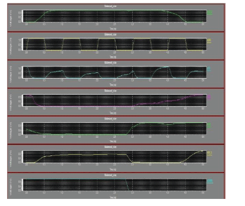
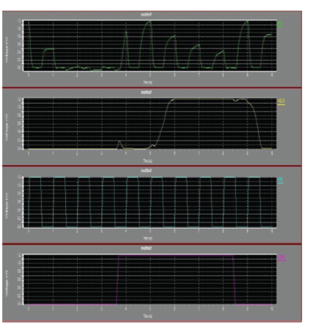
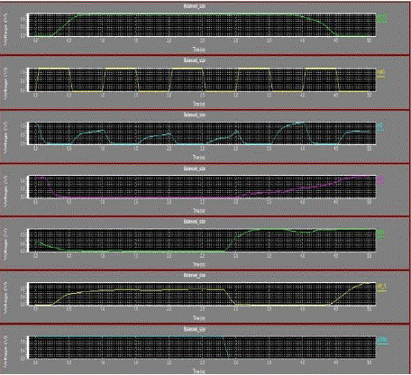
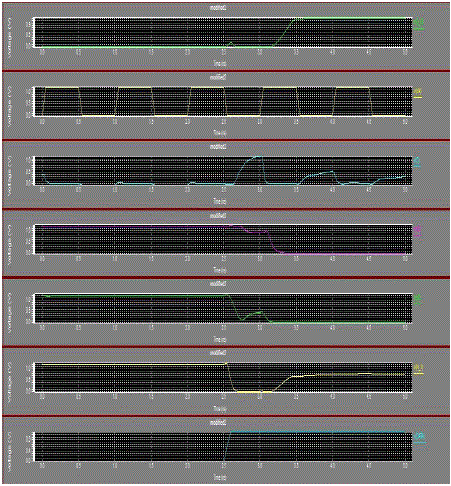
| From the output of DHSCGFF circuit shown in the Fig.5 ,it is analyzed that asynchronous data sampling occurs if D changes when CLK=0 (before falling edge). In the DHSCGFF Balanced Size circuit in Fig.6 is large amount of delay occurs in output and a small error occurs due to asynchronous data sampling problem. If the DHSCGFF Modified-I circuit in Fig.7 is simulated delay occurs in output and error due to asynchronous data sampling problem are removed. In the DHSCGFF Modified-II Size both the delay problem and errors due to asynchronous data sampling problem are completely removed. From the result, it is proved that by modifying the size of transistor in various aspects of Tam’s design reduces the delay and removes Asynchronous Data Sampling. |
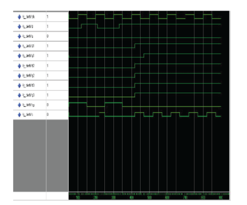
| Simulation result of the asynchronous data sampling with respect to the behavior of the clock signal is shown in the Fig.9 The clk is the clock signal and the other inout signals will have the output as shown. For each simulation, four data switching cases have been tested respectively, from left to right: 1) D changes from 1 to 0 before a falling edge; 2) D changes from 0 to 1 before a rising edge; 3) D changes from 1 to 0 before a rising edge; and 4) D changes from 0 to 1 before a falling edge. The asynchronous transitions have been removed. |
| In the Shift Register built with Serial In Serial Out Configuration using Double Edge Triggered Flip-Flopin Fig.10, the data are shifted in the order of one bit at a time on a single line. It produces the stored information on its output also in serial form. During each clock pulse, one bit is transmitted from left to right and from this output result it is shown the four bits (1010) being serially shifted out of the register and replaced by all zeros. |
CONCLUSION
|
| DETFF and clock gating are two methods to reduce dynamic power consumption, and both of them are successful when used separately. However, when applying clock gating into a DETFF, a data transition error may appear at the output between clock edges due to asynchronous data sampling, which has been defined and discussed. Solution has been provided to avoid the asynchronous sampling problem in clock-gated DETFF. The delay buffer using 4-bit serialin serial-out shift register has implemented for the analysis of asynchronous data sampling. The power comparison between the Shift register implemented using double edge triggered flip-flip and D flip-flop shows that the average power and minimum power consumption of double edge triggered flip-flop is less compared to the implementation of shift register with D flip-flop. Thus the shift register was built using Double Edge Triggered Flip-Flop and the asynchronous data sampling is removed using proposed schemes. |
Tables at a glance
|
 |
 |
| Table 1 |
Table 2 |
|
Figures at a glance
|
 |
 |
 |
 |
 |
| Figure 1 |
Figure 2 |
Figure 3 |
Figure 4 |
Figure 5 |
|
 |
 |
 |
 |
 |
| Figure 6 |
Figure 7 |
Figure 8 |
Figure 9 |
Figure 10 |
|
References
|
- 1 Xiaowen Wang and William H. Robinson, ‘Asynchronous Data Sampling Within Clock-Gated Dual Edge Triggered Flip-Flops’, IEEE Transactions on Circuits and Systems—I: Regular Papers, Vol. 60, pp 2401-2411, 2013.
- W. S. Tam, O. Y. Wong, K. Y. Mok, C. W. Kok, and H. Wong, ‘An energy efficient half-static clock-gating D-type flip-flop’, Int J.Comput.,Syst. and Circuits, vol. 19, no. 3, pp. 635-654, May 2010.
- C.C.Yu,’ Low-power double edge-triggered flip-flop circuit design’, Int. Conf. Innovative Computing Information and Control(ICICIC), p. 566 , 2008
- Wing-Shan Tam, Sik-Lam Siu, Chi-WahKok, and Hei Wong, ‘Double Edge-Triggered Half-Static Clock-Gated D-Type Flip-Flop’, in Int. Conf. Electron Devices and Solid State Circuits, 2010
- A. G. M. Strollo, E. Napoli, and C. Cimino, “Analysis of power dissipation in double edge-triggered flip-flops,” IEEE Trans. Very LargeScale Integr. (VLSI) Syst., vol. 8, no. 5, pp. 624–629, Oct. 2000.
- G. Renganayaki,Jeyakumar.V ‘Design of an Efficient Low power Shift Register using double Edge Triggered Flip-Flop’, International journal of Innovative research in Computer and communication Engineering,vol.2 , Issue 1, pp.2707-2716, Jan 2014
|