International Journal of Advanced Research in Electrical, Electronics and Instrumentation Engineering
ISSN ONLINE(2278-8875) PRINT (2320-3765)
ISSN ONLINE(2278-8875) PRINT (2320-3765)
S.Nandhini1, T.G.Dhaarani1, P.Kokila1 , P.Premkumar1
|
| Related article at Pubmed, Scholar Google |
Visit for more related articles at International Journal of Advanced Research in Electrical, Electronics and Instrumentation Engineering
The full adder design is based upon the split path data driven dynamic logic (PROPAGATE and GENERATE).The adders were characterized for their performance and power consumptions when operated on different supply voltages and fan-outs. This paper involves the reduction in the leakage current and power consumption in the circuit. The static leakage power dissipations can be reduced by supply voltage gating technique which can be done through the transistor, placed between Vdd /Gnd rail and the circuit. This allows the supply voltage to flow through the circuit only during the needed time .As the transistor becomes ON condition then only the power is applied to the circuit. By this method the static power gets reduced and the speed of the process also improved with high drivability with comparing to the conventional dynamic domino adders. By this technique of reducing the leakage power, the expecting power consumption is about 30% less than the existing method .Thus the newly designed full adder with reduced power consumption is implemented in the array multiplier for better performance.
Keywords |
| Full Adder, Supply voltage gating, Multipliers, Tanner EDA. |
I.INTRODUCTION |
| The Demand and popularity of portable electronics is driving designers to strive for smaller silicon area, higher speeds, longer battery life, and more reliability. Power is one of the premium resources a designer tries to save when designing a system. Full adders are fundamental units in various circuits, especially in circuits used for performing arithmetic operations such as compressors, comparators, parity checkers, and so on [3]. Full adders are often in the critical paths of complex arithmetic circuits for multiplication and division. These in turn form the core of any system and thereby influence the overall performance of the entire system. Enhancing the performance of the full adder can significantly affect the system performance. Fig 1.2 shows the power consumption breakdown in a modern day high-performance microprocessor [2]. It includes various units such as control unit, memory unit, clock cycles and data path as the basic functions of the processors. |
| The data path consumes roughly 30% of the total power of the system. Adders are an extensively used component in data paths and, therefore, careful design and analysis is required for these units to obtain optimum performance. At the circuit level, an optimized design is desired to avoid any degradation in the output voltage, consume less power, have less delay in critical path, and be reliable even at low supply voltage as we scale towards deep sub micrometer. Good driving capability under different load conditions and balanced output to avoid glitches is also an important virtue. Since the full-adder cells are duplicated in large numbers, layout regularity, and interconnect complexity are also important. |
| At the circuit level, an optimized design is desired to avoid any degradation in the output voltage, consume less power, have less delay in critical path, and be reliable even at low supply voltage as we scale towards deep sub micrometer. Good driving capability under different load conditions and balanced output to avoid glitches is also an important virtue. Since the full-adder cells are duplicated in large numbers, layout regularity, and interconnect complexity are also important. Several logic styles have been used in the past to design full adder cells. Each design style has its own merits and demerits. Classical designs of full adders normally use only one logic style for the whole full-adder design. |
II.RELATED WORKS |
| The existing methodology includes three new full adder circuits using the recently proposed split-path data driven dynamic logic. In this an exploratory study of popular adder structures implemented in the IBM 90-nm process and analysed for performance, power, area, fan-in, fan-out, and process and voltage variations. Based on the logic function realized, the adders were characterized for performance and power consumption when operated under various supply voltages and fan-out loads and the impact of sum and carry propagation delays on the performance, power of these systems[1]. Three different adder functions were also realized using the recently proposed Data Driven Dynamic Logic (D3L) and split-pre Charge Data Driven Dynamic Logic (sp-D3L). |
| The performance of a full adder circuit depends to a great extent on the type of design style used for implementation as well as the logic function realized using the particular design style. For instance, a standard CMOS implementation allows circuits to achieve a reasonable Power Delay Product (PDP)[2] with high noise margins, regular layout and relatively higher tolerance to process variations. Dynamic implementations on the other hand may yield an extremely fast design but end up paying higher costs in the overall power consumption. D3L and sp-D3L[9] are two design styles which allow high performance dynamic circuit design without the additional power consumption in the clock distribution network. Thus these styles form interesting implementation strategies for realizing high performance, power-efficient full adders. |
| In addition to the logic function and implementation style, the sizing of the transistors also plays an extremely important role in the optimization of circuit performance, power consumption, noise margins, fan-in, fan-out, etc. For dynamic adders it was observed that progressively sizing the rest of the transistors yielded the best power-delay product while also maintaining drivability of the adder circuits. It was observed that progressive sizing of transistors yielded the best power-delay product for each of the adder circuits considered. As a result, all the adders were sized accordingly.[3] For the pass-transistor and transmission gate based adders i.e. adders without drivability, we kept minimum sizes on all the transistors. |
| Hence, minimum sizing all the transistors yielded the best power-performance and area trade off. The delays reported correspond to the worst case delays observed in every adder. It can be seen that the hybrid adder provides the best PDP amongst all the adders when simulated standalone. The full adder functions characterized using the sp-D3L methodology provide the lowest delay with the adder working almost twice as fast as the standard adders selected in the study. The drawback of these adders is of course the high power consumption, due to the large number of transistors as well as the multiple paths to ground present in the sp-D3L implementations[5]. With respect to the choice of logic function to implement, the full adder was observed to perform the best when implemented using the PROPAGATE and GENERATE signals.This can be attributed to the fact that this function allows for smaller number of transistors stacked in series and shows the lowest capacitance at the output node. This shows that the capacitance at the output node forms the most critical component of the adder speed irrespective of the number of stages of circuits before getting the SUM and CARRY outputs. |
| On a functional level, it can be observed that once again the adders based on the PROPAGATE, GENERATE signals fare the best. Especially in the D3L [5] andsp-D3L [9] implementations of this function, this performance advantage can be attributed to the periodic refreshing of voltage levels between the intermediate adder stages. These adders however continue to suffer from high power dissipation, most possibly due to the large number of switching nodes, and increased short-circuit power dissipation with increased loading[10]. |
III. PROPOSED SYSTEM |
| In the proposed method the static loss in the circuit can be reduced by using the supply voltage gating technique. In this method the voltage drop can be reduced by connecting two transistors between the Vdd/gnd rail and the circuit. This allows the supply voltage to flow through the circuit only during the needed time .As the transistor becomes ON condition then only the power is applied to the circuit. By this method the static power gets reduced and the speed of the process also improved with high drivability with comparing to the conventional dynamic domino adders. |
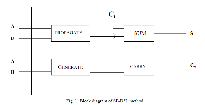 |
| In the Fig. 1, the adder module is formed by the major blocks known as propagate and generate. The propagate output is formed by the XOR of two inputs A and B as . The generate output is formed by the AND operation between the two inputs A and B as A.B. The SUM output is formed by the XOR operation of propagate output and the input Ci. The Cout is obtained by the OR operation between the propagate output and the product of propagate output and Ci input. The performance of a full adder circuit depends to a great extent on the type of design style used for implementation as well as the logic function realized using the particular design style. |
| For instance, a standard CMOS implementation allows circuits to achieve a reasonable Power Delay Product (PDP) with high noise margins, regular layout and relatively higher tolerance to process variations. Dynamic implementations on the other hand may yield an extremely fast design but end up paying higher costs in the overall power consumption. D3L and sp-D3L are two design styles which allow high performance dynamic circuit design without the additional power consumption in the clock distribution network. Thus these styles form interesting implementation strategies for realizing high performance, power-efficient full adders. |
| In addition to the logic function and implementation style, the sizing of the transistors also plays an extremely important role in the optimization of circuit performance, power consumption, noise margins, fan-in, fan-out, etc. For dynamic adders it was observed that progressively sizing the rest of the transistors yielded the best power-delay product while also maintaining drivability of the adder circuits. |
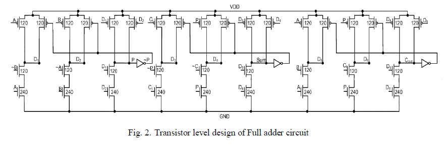 |
| Fig . 2 shows the full adder implementation in sp-D3L design style. It was observed that progressive sizing of transistors yielded the best power-delay product for each of the adder circuits considered. As a result, all the adders were sized accordingly. For the pass-transistor [8] and transmission gate [11] based adders i.e. adders without drivability, we kept minimum sizes on all the transistors. Hence, minimum sizing all the transistors yielded the best power-performance and area tradeoff. Three different adders were realized under recently proposed data Driven Dynamic Logic (D3L) and split path Data Driven Dynamic Logic (sp-D3L). |
| SPLIT PATH DATA DRIVEN DYNAMIC LOGIC (sp-D3L) |
| A new dynamic logic named split-path D3L (spD3L) [5] that overcomes the speed limitations of D3L. The split path D3Ldesign style derived from standard D3L allows the design of high speed dynamic circuits without the power overhead of the clock tree while providing significantly higher performance than the D3L due to reduced capacitance at the pre-charge node. To demonstrate the performance benefits of the new split-path dynamic approach, the proposed adder with conventional static and dynamic adder cells are used. All the adder circuits were characterized for speed, power, area, noise margins; supply voltage scaling as well as fan-out capabilities. |
| To evaluate the combined impact of load driven by the adder and load presented by the adder to the driving circuit, a combined fan-in fan-out analysis with varying loads was also performed. The new design was found to achieve from16% to 27% performance advantages over its static and dynamic counterparts at nominal supply voltage. With supply voltage scaled from 1 V to 0.8 V, the adder shows 12%, 34% and 39% PDP advantage over domino, static and conventional D3L designs respectively. Fan-out analysis showed the adder to perform with 11% to 41% better PDP than the others. |
| POWER GATING |
| This technique uses high Vt sleep transistors which cut off VDD from a circuit block when the block is not switching. The sleep transistor sizing is an important design parameter. This technique, also known as MTCMOS or Multi- Threshold CMOS reduces stand-by or leakage power. Power gating [1] affects design architecture more than clock gating. It increases time delays as power gated modes have to be safely entered and exited. |
| Architectural trade-offs exist between designing for the amount of leakage power saving in low power modes and the energy dissipation to enter and exit the low power modes. Shutting down the blocks can be accomplished either by software or hardware. Driver software can schedule the power down operations. Hardware timers can be utilized. A dedicated power management controller is another option. An externally switched power supply is a very basic form of power gating to achieve long term leakage power reduction[12]. |
| To shut off the block for small intervals of time, internal power gating is more suitable. CMOS switches that provide power to the circuitry are controlled by power gating controllers. Outputs of the power gated block discharge slowly. Hence output voltage levels spend more time in threshold voltage level. This can lead to larger short circuit current. Power gating uses low-leakage PMOS transistors as header switches to shut off power supplies to parts of a design in standby or sleep mode. |
| NMOS footer switches can also be used as sleep transistors. Inserting the sleep transistors splits the chip's power network into a permanent power network connected to the power supply and a virtual power network that drives the cells and can be turned off. The quality of this complex power network is critical to the success of a power-gating design. Two of the most critical parameters are the IR-drop and the penalties in silicon area and routing resources. Power gating can be implemented using cell- or cluster-based (or fine grain) approaches or a distributed coarse-grained approach. |
| POWER GATING PARAMETERS |
| Power gating implementation has additional considerations for timing closure implementation. The following parameters need to be considered and their values carefully chosen for a successful implementation of this methodology. |
| Power gate size: The power gate size must be selected to handle the amount of switching current at any given time. The gate must be bigger such that there is no measurable voltage (IR) drop due to the gate. As a rule of thumb, the gate size is selected to be around 3 times the switching capacitance. Designers can also choose between header (P-MOS) or footer (N-MOS) gate. Usually footer gates tend to be smaller in area for the same switching current. Dynamic power analysis tools can accurately measure the switching current and also predict the size for the power gate. |
| Gate control slew rate: In power gating, this is an important parameter that determines the power gating efficiency. When the slew rate is large, it takes more time to switch off and switch-on the circuit and hence can affect the power gating efficiency. Slew rate is controlled through buffering the gate control signal. |
| Simultaneous switching capacitance: This important constraint refers to the amount of circuit that can be switched simultaneously without affecting the power network integrity. If a large amount of the circuit is switched simultaneously, the resulting "rush current" can compromise the power network integrity. The circuit needs to be switched in stages in order to prevent this. |
| Power gate leakage: Since power gates are made of active transistors, leakage reduction is an important consideration to maximize power savings. |
IV. RESULTS AND DISCUSSIONS |
| TANNER EDA |
| Tanner EDA is a leading provider of Electronic Design Automation (EDA) software solutions for the design, layout and verification of analog/Mixed Signal ICs and MEMs. This tool helps to automate and simplify the design process,enabling engineers to cost-effectively bring commercially successful electronic products to market ahead of the competition. |
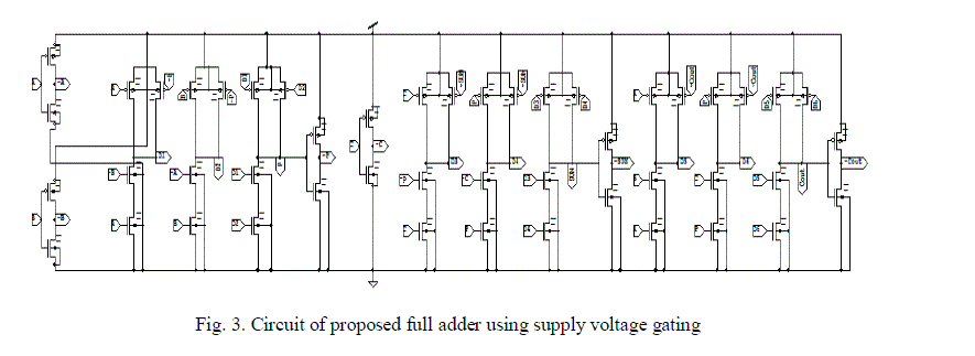 |
| Fig. 3 shows the implementation of the proposed full adder system by the combination of SUM and PROPAGATE blocks. The generate output is formed by the AND operation between the two inputs A and B as A.B. The SUM output is formed by the XOR operation of propagate output and the input Ci. The Cout is obtained by the OR operation between the propagate output and the product of propagate output and Ci input. |
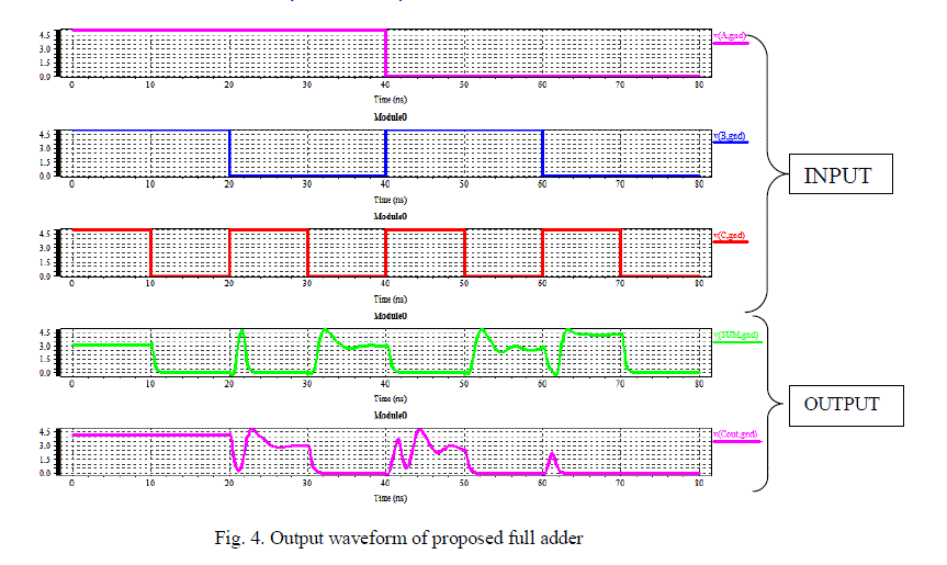 |
| Fig. 4 represents the simulation output waveform for proposed full adder system in the T-spice input window through which the inputs for the SUM and PROPAGATE circuit section and other commands functions are inserted using INSERT COMMAND option present in T-spice. The clocked-PMOS transistor ON during the pre charge phase and it sets the dynamic node to the logic value “1”. During the evaluation phase, whereas the clocked-NMOS transistor (the so-called footer transistor) is ON providing the evaluation network with a path to ground. |
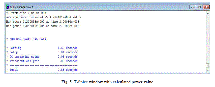 |
| Fig. 5 shows T spice window with the calculated power value. It has been found that the power consumed by a proposed full adder using supply voltage gating in Tanner EDA Tool was 2.00084 e-008. The simulated data presented is obtained using the Tanner EDA Tool and executed for a 90nm CMOS process. The dynamic power consumption is reduced significantly with reduced supply voltage. |
VI.CONCLUSION |
| On regards of the simulation, it can be seen that the proposed full-adders require low power than the existing method. Actual power consumed is around 30% of the previous method. And by using power gating technique the power can be minimized to some extent which enhances the performance of the full adder circuit. Thus by using the proposed full adder, the array multiplier can be designed and the performance of the array multiplier can also be improved. |
References |
|