Keywords
|
| Low-noise amplifier (LNA), Radio Frequency (RF) and CMOS, Single stage amplifier, Active Passive component, RF front end. |
INTRODUCTION
|
| In past time amplifiers play very important role for the signal amplification in communication systems and in the receiver design but as the demand of accuracy, timing increasing the demand of a amplifier increasing which may perform multiple operations at a single time this is possible by the Low noise amplifier such as amplification of weak signal, reduction of noise, reduce noise figure, increased gain and power level high stability, improve voice and data quality and eliminate channel interference, an additional feature of LNA is to amplify the signal and reduce the noise in the signal at the same time. In the communication market the demand of LNA is increasing with increasing the market of Cell Phones, GPS, and Bluetooth etc, which is used in day to day life. A Low Noise Amplifier is the basic building block of any communication system. It is placed at the front end of a radio receiver and works as an electronic amplifier to amplify the received signals to acceptable levels with minimum self generated additional noise while radio receiver composed of amplifier, mixer and filter. The first part is an LNA which is the most important part of the receiver. The main function of LNA is to amplify extremely low signals without adding noise thus preserving required signal to noise ratio at extremely low power level and large signal levels and provides first level of the amplification that can be received by the receiver is the receiver’s sensitivity also. It amplifies the received signal without introducing any distortions hence eliminating channel interference. The dynamic range of the receiver which is the difference between the largest possible received signal and the small possible received signal is defining the quality of receiver chain. The largest signal that can be received by the receiver establishes an upper power level limit that can be handled by the system while preserving voice or data quality. The reasons behind using LNA are signal coming from the antenna is very small, amplification of the signal is needed, reasonable or minimum power consuming gain, noise figure, non linearity and impedance matching are the most important parameters in LNA design. An LNA is a design that minimizes the noise figure of the system by matching the device to its noise matching impedance. As we see the role of LNA in Radio receiver that LNA amplify received signal, boost the desired signal power, reduced noise in the receiver, increased gain in the receiver. An amplifier which uses is the single stage amplifier. |
| This paper indicates the background information of radio receiver. In this configuration first we design a low noise amplifier, second mixer and third filter. The first stage of a receiver is typically a low-noise amplifier (LNA), whose main function is to provide enough gain to overcome the noise of subsequent stages (for example, in the mixer or IF amplifier). Aside from providing enough gain while adding as little noise as possible, an LNA should accommodate large signals without distortion, offer a large dynamic range, and present good matching to its input and output, which is extremely important if a passive band select filter and image-reject filter precedes and succeeds the LNA, since the transfer characteristics of many filters are quite sensitive to the quality of the termination. LNA schematic is a basic circuit design to represent the elements of the system. LNA schematic combines both of the Common and Cascade LNA. This is used to find out the results of LNA. |
RADIO RECEIVER ARCHITECTURE AND ROLE OF LNA
|
| In radio communications, a radio receiver is an electronic device that receives radio waves and converts the information carried by them to a usable form. It is used with an antenna. The antenna intercepts radio waves (electromagnetic waves) and converts them to tiny alternating currents which are applied to the receiver, and the receiver extracts the desired information. The receiver uses electronic filters to separate the wanted radio frequency signal from all other signals, an electronic amplifier to increase the power of the signal for further processing, and finally recovers the desired information through demodulation. The information produced by the receiver may be in the form of sound (an audio signal), images (a video signal) or data (a digital signal) [2]. A radio receiver may be a separate piece of electronic equipment, or an electronic circuit within another device. Devices that contain radio receivers include television sets, radar equipment, two way radio, cell phone, wireless computer networks, GPS navigation devices, satellite dishes, radio telescope, Bluetooth enabled device, garage door openers, and baby monitors. |
| Alexander Stepanovich Popov designed and implemented the first radio receiver in 1896. The radio receiver has seen a great many technological advances. One of the most significant advances was the invention of the super heterodyne, or superhet, receiver. The receiver demodulates and decodes the channel output to recover the original information to the source. Once demodulated, the channel decoder, which is typically a filter matched to the channel encoder, is used to recover one sample estimate per symbol of the channel code word. The channel encoder estimate the digital source code word, which is then converted to an estimate the original data by the source decoder. |
| Heterodyne architecture is probably the most commonly used receiver in current commercial receiver implementation. The low noise amplifier plays a key role in this architecture. The main objective of the super heterodyne receiver is to produce an intermediate frequency (IF) by the process of heterodyning or beating. This can be accomplished when two frequencies are mixed to produce the beat frequency. |
| The first stage of a receiver is typically a low-noise amplifier (LNA), whose main function is to provide enough gain to overcome the noise of subsequent stages (for example, in the mixer or IF amplifier). Aside from providing enough gain while adding as little noise as possible, an LNA should accommodate large signals without distortion, offer a large dynamic range, and present good matching to its input and output, which is extremely important if a passive band select filter and image-reject filter precedes and succeeds the LNA, since the transfer characteristics of many filters are quite sensitive to the quality of the termination. Figure1 shows the architecture of heterodyne receiver using LNA. The band-select filter before the LNA rejects the out-of-band interferers. The image reject filter (preselected) after the LNA attenuates the image which is 2ωIF away from the desired band [3]. |
DESIGN AND ARCHITECTURE OF LOW NOISE AMPLIFIER
|
| The low noise amplifier is an electronic amplifier used to amplify possibly very weak signals. It is usually located very close to the detection device to reduce losses in the feed line of any amplifier. An LNA is a key component which is placed at the front –end of a radio receiver circuit. Using an LNA, the effect of noise from subsequent stages of the receiver chain is reduced by the gain of the LNA, while the noise of LNA itself is injected directly into the received signal. Low Noise Amplifier represents one of the basic building blocks of the communication system. The purpose of the LNA is to amplify the received signal to acceptable levels while minimizing the noise it adds. A good LNA has a low NF (like 1dB), a large enough gain (like 20 dB)and should have large enough inter modulation and compression point (IP3 and P1dB). Further criteria are operating bandwidth, gain flatness, stability, input and output VSWR In the design of LNA another consideration is to choose the single ended or differential architecture. The single ended configuration provides a lower noise figure whereas both the branches contribute to the noise at the output in differential configuration. Additionally, the current in each transistor in the differential circuit is half that of the single-ended topology. The transit frequency of the device would be smaller for the differential circuit, which degrades the noise figure of the circuit. But the differential topology can provide an increased output dynamic range and also a better tolerance to commonmode interferences in the circuit. Due to the differential nature of the circuit the effect of the parasitic inductance of the ground pin is reduced. There are several advantages in using a differential design. Firstly, the virtual ground formed at the ‘tail’ removes the sensitivity to parasitic ground inductances, which makes the real part of the input impedance purely controlled by the source degeneration inductance (Ls). Secondly the differential amplification of the signal ensures an attenuation of the common mode signal, in most of the system this common mode signal will be noise. Thirdly, the use of Gilbert mixers and image rejection schemes require to be fed from a differential source [10]. |
STANDARD LNA FEATURES AND CHARECTERSTIS
|
| There are some important features that should consist with a Low Noise Amplifier: |
| A. Operating supply voltage: Usually a Low Noise Amplifier require less operating voltage in the range of 2 to 10 V.MAX 2640 operates at 2.7 to 5.5V. |
| B. Operating Supply current: LNA require supply current in the range of mA,the supply currentrequire for LNA is dependent on its design and the application for which it has to be used. MAX 2640 which is used for satellite application requires a supply current of nearly 6mA. |
| C. Operating Frequency: For LNA design Frequency range is to be decided between 500KHz to 50 GHz. |
| D. Operaing Noise Figure: Noise Figure determines efficiency of an LNA,hence we can decide which LNA is suitable for an LNA is suitable for a particular application.For example in satellite communication ,an LNA having a very low noise figure is required.Mac 2640 which is used for communication purpose have noise figure in the range 0.9-1.5dB. |
| E. Operating Temperature Range: LNA has some limit on its operating temperature,General range for faithful operation of LNA is -30 ºC to +50 ºC, MAX 2640 operates on very wide temperature range i.e. -40 to +125 ºC. |
LNA DESIGN PROCESS
|
| There are many types of LNA ‘s available in the market but we used Common and Cascode LNA composed these two and make a new architure that contain excellent input output impedance matching and high gain. |
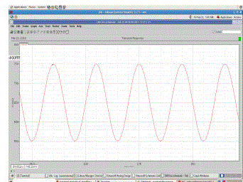
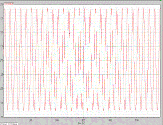
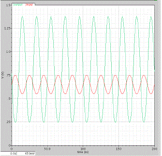
| First for the LNA Schematic we apply 1.8V Input Voltage ,waveforms for an input voltage are shown in figure. |
| Supply Current that we give is 2.66mA,this range of current is applying specially for choosing of LNA for the designing of UWB Radio Receiver. |
1. Common LNA
|
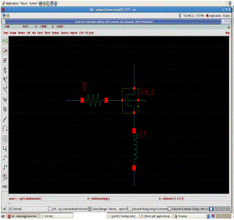
| First we design the Common gate amplifier using the Cadence Tool Shows gate as an input signal and drain as an output signal.It is useful ,for example CMOS RF receiver especially when operating near the frequency limitations of FET.It is desirable because of the ease of impedance matching and potentially has lower noise. |
2. Cascode LNA
|
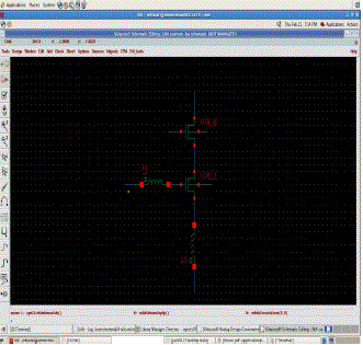
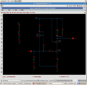
| The cascade of CS Stage and CG Stage is called cascade. In Cascode LNA two transistor M1 and transistor M2 is used both are connected in series and two inductors L1 and L2 is connected to both of these. We have used Cadence Virtuoso (R) Schematic XL Tool for design of Low Noise Amplifier. |
| We have a coparison among different types of an LNA,this concept to choose a common LNA for Excellent Input matching and cascade LNA for High Gain. |
LNA SCHEMATIC AND SIMULATION
|
| The CADENCE environment allows access to libraries containing icons of basic circuit components and the ability to place and connect theses devices in the form of a circuit within a schematic editor. In addition, the default values of the properties of the various elements can be edited and altered to fit the requirements of the actual system under design. The files can then be extracted from the graphical circuits into forms compatible with Spectra or Spice circuit simulators. The LNA usually only involves one or two transistors to achieve low noise operation. The performance of the LNA circuits is very dependent on process technology. CMOS technologies are the best choice to design an LNA because they offer high speed operation, simplicity in fabrication, and low power consumption. |
| The approach used in the redesign and simulation includes next steps: |
| • S-parameters simulation of the LNA scheme realized in 0.18μm CMOS technology; |
| • Drawing the LNA scheme in 0.18μm CMOS technology |
| Simulation software allows for modeling of circuit operation and is an invaluable analysis tool. The simulators can then be called to compute and plot the various waveform results. Once the designer is satisfied with the operation of the circuit, the schematic can then be put into the form of a symbol and used as a component in higher-level circuits. In LNA design presents a considerable challenge because of its simulations requirement for high gain, low noise figure, good input and output matching and unconditional stability at the lowest possible current draw from the amplifier. The LNA is required to amplify incoming signals and extract them from the noisy environment. |
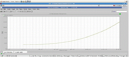
| CMOS LNA designed using 0.18μm UMC technology using 1.8 V supply voltage, current 2.66mA. So we can find the power will be 4.7mW. voltage gain will be 15.04 dB at 8.72 GHz frequency. |
| The overall noise figure is mainly determined by the first amplification stage, provided that it has sufficient gain. NF is the practical noise figure of a practical RF network and NFmin is the ideal or a theoretical noise figure of a circuit, NF = NFmin + matched network factor. |
APPLICATIONS OF LOW NOISE AMPLIFIER
|
| LNA is broadly applicable as an enhancing or even enabling technology within biotechnology, molecular biology research and drug development.Other Application of a low noise amplifier is as follows. |
| (i) ISM Radios-The industrial, scientific and medical radio bands (portions of the radio spectrum) reserved internationally for the use of radio frequency (RF) energy for industrial, scientific and medical purposes other than communications. Examples of applications in these bands include radio frequency process heating, microwave ovens, and medical diathermy machines. |
| (ii) GPS Receiver- Global Positioning System is a space-based satellite navigation system that provides location and time information in all weather conditions, anywhere on or near the Earth where there is an unobstructed line of sight to four or more GPS satellites. The system provides critical capabilities to military, civil and commercial users around the world. |
| (iii) Wireless LAN- wireless local area network links two or more devices using any wireless distribution method (typically spread-spectrum or OFDM radio), and usually providing a connection through an access point to the wider Internet. |
| (iv) Automotive RKE- A remote keyless entry system used to gain entry to automobiles. In optics, RKE may refer to a type of Eyepiece. |
| (v) Satellite Communication- In a satellite communications system, the ground station receiving antenna will connect to a LNA. The LNA is needed because the received signal is weak; it is usually a little above the noise floor. |
LNA RESULT
|
| As LNA is very important for Radio Reciver design (specially UWB Radio Receivers) and other application also wide work has been done on LNA, many important factors are associated, LNA is designed at different frequency ranges for weak signals amplification as the frequency is different the effect is on the signal amplification and other parameters such as noise figure,gain,impedance matching. |
ACKNOWLEDGEMENT
|
| I extend my sincere and heart felt thanks to Ms. Suraj Sharma my project guide for providing me the right ambience for carrying out this work on “Design of Low Noise Amplifier for UWB Radio Receiver” and its application when it is still a new and unproven field as well as for their support, encouragement and facilities in completing this project. I am profoundly indebted to Mr. Manhar Tiwari and special thanks to Mr. Akshat Gupta for innumerable acts of timely encouragement and advice. |
Tables at a glance
|
|
|
Figures at a glance
|
 |
 |
 |
 |
 |
| Figure 1 |
Figure 2 |
Figure 3 |
Figure 4 |
Figure 5 |
|
 |
 |
 |
 |
| Figure 6 |
Figure 7 |
Figure 8 |
Figure 9 |
|
References
|
- Thomas H. Lee “The Design of CMOS Radio Frequency Integrated Circuits”, Cambridge University Press, 1998.
- Ulrich L. Rohde, Jerry Whitaker “Communications Receivers” Third Edition, McGraw Hill, New York, 2001, ISBN 0-07-136121-9.
- Buscarcopias de Dr. Jimenez en Reproducciones ($1-$2) – “Digital circuits using MOS transistors”
- H. C. Lin and L.W. Linholm, “An optimized output stage for MOS integrated circuits,” IEEE Journal of Solid-State Circuits, vol. 10, pp. 106–109,April 1975.
- R. C. Jaeger, “Comments on An optimized output stage for MOS integrated circuits,” IEEE Journal of Solid-State Circuits, vol. 10, pp. 185–186, June1975.
- B. Razavi, “Design of Analog CMOS Integrated Circuits”, McGraw-Hill, 2001.
- Guillermo Gonzalez, “Microwave Transistor Amplifiers”, Prentice Hall, 1984.
- LNA Design Using Spectra RF Application Note Product Version 5.0 December 2003 September by Cadence Design Systems.
- Reinhold Ludvig, PavelBretchko: RF Circuit Design - Theory and Applications, Prentice Hall 2000, ISBN 0-13-095323-7.
- R. Ramazan, “Tutorial simulation of LNA”, Linkoeping University, Sweden, 2009.
- T.H. Lee, the Design of Cmos Radio - Frequency Integrated Circuits, Cambridge University, 2004.
- Sungkyung Park and Wonchan Kim, “Design of a 1.8 GHz low-noise amplifier for RF front-end,”Consumer Electronics, IEEE Transactions on, vol.47, no. 0098, 2001.
- D. K. Shaeffer, T. Lee, “A 1.5V, 1.5GHz CMOS Low Noise Amplifier,” IEEE Journal of Solid-State Circuits, vol. 32 no.5 May 1997.
- B. Razavi, “CMOS Technology Characterization for Analog and RF Design,” IEEE Journal of Solid-State Circuits, vol. 34, no. 3, March. 1999.
- Adel S. Sedra and Kenneth C. Smith, Microelectronic Circuits, 1987, Holt, Rinehart and Winston, Inc.
- Worcester Polytechnic Institute. “Cadence Design Tools Tutorial”.http://turquoise.wpi.edu/cds/examples/layout.4.html
- Ahmad Saghafi; AbdolrezaNabavi(2006) “An Ultra-Wideband Low-Noise Amplifier for 3–5-GHz Wireless Systems” 18th International Conferenceon Microelectronics (ICM) 2006.
- Pablo M. G.; Mohammad H.(2006) “Design of a CMOS Low-Noise Amplifier” ,Stanford University
- ZHANG H.; CHEN Gui;(2008) “Design of a fully differential CMOS LNA for 3.1–10.6 GHz UWB communication systems”.
- J.P.Silver, “ MOS Differential LNA design Tutorial”.
- Reza Molavi (2005) On “The design of Wideband CMOS Low-Noise Amplifiers”.
- NackgyunSeong, Yohan Jang, and Jaehoon Choi, (2011) “Design And Analysis Of A Compact Ultra- Wideband CMOS Low-Noise Amplifier,”Microwave And Optical Technology Letters, Vol. 53, No. 2, pp. 345-348.
- Yi-Jing Lin, Shawn S. H. Hsu, Jun-De Jin, and C. Y. Chan (2007): “A 3.1–10.6 GHz Ultra-Wideband CMOS Low Noise Amplifier With Current-Reused Technique,” IEEE Microwave And Wireless Components Letters, Vol. 17, No. 3.
|