Keywords
|
| Low Power, SAR ADC, Comparator, Biomedical Applications |
INTRODUCTION
|
| Analog to Digital Converters are important building blocks in lots of applications. In past few years, more and more applications are built with very stringent requirements on power consumption. For electronic systems, such as wireless systems or implantable devices, the power consumption is becoming one of the most critical factors. The stringent requirements on the energy consumption increase the need for the development of low voltage and low power circuit techniques and system building blocks. |
| Analog-to-Digital Converters (ADCs) translate the analog quantities into digital language, used in information processing, computing, data transmission and control systems. ADCs are key components for the design of power limited systems, in order to keep the power consumption as low as possible. Implantable Medical electronics, such as Pacemakers and cardiac defibrillators are typical examples of devices where ultra-low-power consumption is paramount .The implanted units rely on a small non rechargeable battery to sustain a lifespan of upto10years. |
| The life time of the artificial pacemakers should last up to 10 years which mandate low power consumption per operation. The analog to digital converter is the crucial part of an implantable pacemaker since it consumes a large amount of power as the interface between sensed analog signal and digital signal processor block. Therefore, decreasing the power consumption of the ADC is a major concern. |
| Low power ADCs with moderate resolution and low sampling frequency is suited for biomedical application. These specifications make SAR ADC the suitable choice. It consumes low power due to its simple structure. Moreover, SAR ADC is scalable with the technology scaling since most parts of the architecture apart from the comparator are digital. |
PACEMAKER OPERATION
|
|
| Pacemakers directly control the pattern and speed of the heartbeat. When the heart stops beating or it beats too slowly, pacemaker provides weak electrical signals with approximately 70 beats per minute to correct the timing of the heart beat. This medical device contains a battery, a generator and pacing leads. The leads connect the pacemaker to the heart and stimulate the heart with the pulses generated in pacemaker. Battery and generator are inside a titanium container which is placed inside the body. |
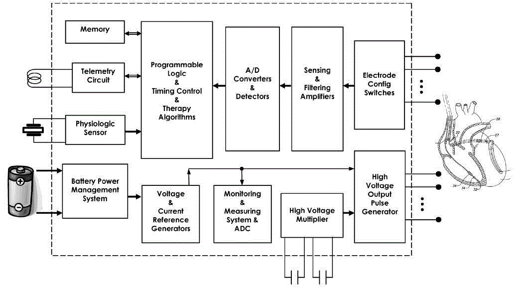
| Figure shows the block diagram of a pacemaker. The main blocks fall into four parts |
| 1) At the input, there are sensing system, amplifier, filter, and analog to digital converter. |
| 2) The digital output of the ADC is fed to the logic block |
| This consists of a programmable logic, timing control system and therapy algorithms. |
| 3) Current and voltage reference generator and battery power management. |
| 4) At the output of the pacemaker, high voltage pulse generator and multiplier exist. |
SUCCESSIVE APPROXIMATION ADC
|
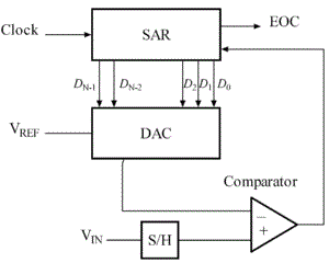
| This section describes different components of SAR ADC architecture. The main components of SAR ADC are a Sample and Hold, a Digital to Analog Converter (DAC), a Comparator and a SAR Logic. |
| A) OPERATIONAL AMPLIFIER: |
| The main building block of analog circuit design is the operational amplifier (op amp). Its primary use is to provide sufficient gain and to implement all analog signal processing functions using negative feedback. Such analog signal processing functions include amplification, integration, filtering, and summation. Op-amps with vastly different level of complexity are used to realize functions ranging from dc bias generation to high gain amplification, filtering or ADCs. |
| B) SAMPLE AND HOLD: |
| The Sample & Hold uses a capacitor and an analog switch to connect or isolate the capacitor from the input. An operational amplifier connected as follower avoids the effects of the load. The amplifier can be powered down in order to reduce the power consumption when the circuit is in the standby mode. |
| The most basic form of the sample and hold circuit combines a switch and a capacitor, the operation of the circuit as follows. In sampling mode the switch is “on”, creating the signal path that allows the capacitor to track an input voltage. When the switch is “off” an open circuit is created that isolates the capacitor from the input, hence changing the circuit from sampling mode into holding mode. |
| C) COMPARATOR |
| The comparator is an essential part in the SAR ADC to perform the binary search algorithm. Comparator in the SAR ADC takes more power consumption than the other blocks. A comparator generates a logic output high or low based on the comparison of the analog input with a reference voltage. |
| In an ideal comparator, with infinite gain, for input voltages higher than the reference voltage, the comparator outputs logical one and for the input voltages lower than the reference voltage it produces zero at the output. |
| D) DIGITAL TO ANALOG CONVERTER |
| The Digital to Analog Converter has a resolution of 8 bits. The converter has been divided into two 4 bits D/A converters to reduce the total area. Each block can be powered down independently to reduce the power consumption. |
| In this architecture we are using R-2R ladder network DAC. The advantage of the R-2R ladder method is only two values of resistors are used greatly simplifying the task of matching or trimming and temperature tracking. Since the output of the R-2R DAC is the product of the reference voltage & digital input word, the R-2R ladder DAC is often called as MDAC. |
| E) SAR LOGIC |
| Successive Approximation Register (SAR) control logic determines each bit successively. The SA register contains N bit for an N-bit ADC. There are 3 possibilities for each bit, it can be set to „1?, reset to „0? or keeps its value. In the first step, MSB is set to „1? and other bits are reset to „0?, the digital word is converted to the analog value through DAC. The analog signal at the output of the DAC is inserted to the input of the comparator and is compared to the sampled input. |
| Based on the comparator result, the SAR controller defines the MSB value. If the input is higher than the output of the DAC, the MSB remains at „1?, otherwise it is reset to „0?. The rest of bits are determined in the same manner. In the last cycle, the converted digital word is stored. Therefore, an N-bit SAR ADC takes N+1 clock cycles to perform a conversion. |
| Successive approximation register ADC implements the binary search algorithm using SAR control logic. In general, there are mainly two fundamentally different approaches to designing the SAR logic. The first one which is proposed by Anderson consists of a ring counter and a shift register. At least 2N flip flops are employed in this kind of SAR. The other, which is proposed by Rossi, contains N flip flops and some combinational logic. |
EXPERIMENTAL RESULTS
|
| A) OPERATIONAL AMPLIFIER: |
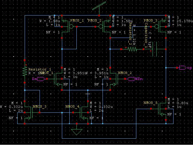
| The first aspect considered in the design was the specifications to be met. Based on a clear understanding of the specifications, the circuit topology of the standard CMOS operational amplifier was chosen because it was believed that such a design could meet the specifications and that the design of such an amplifier is fairly simple. |
| In the above NIN is the non inverting terminal, IN is inverting terminal and OP is the output terminal of the op-amp. |
| B) SAMPLE & HOLD |
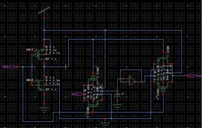
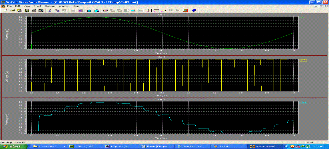
| In below figure voltage follower is placed after the capacitor in order to avoid the loading effect on the capacitor. The S/H operation is conceptually illustrated by the circuit shown. The opening and closing of the switch or sampler is controlled by a sample command (i.e., clock) . |
| When the switch is closed (clk=„1?), the capacitor C charges that is samples and tracks the input signal. When the switch opened (clk=?0?), the output is held at the voltage that the capacitor is charged to at Vo, until the next sampling pulse arrives (clk=?1?). The time interval during which the sampler is closed is called the sampling duration period P. |
| C) COMPARATOR |
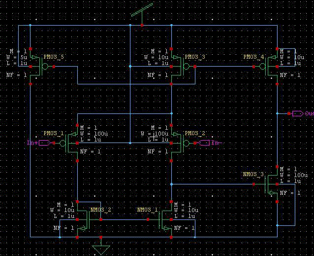
| A comparator generates a logic output high or low based on the comparison of the analog input with a reference voltage. The comparator in the SAR ADC takes more power consumption than other blocks. In SAR ADC we must design comparator such that it consumes very less power. |
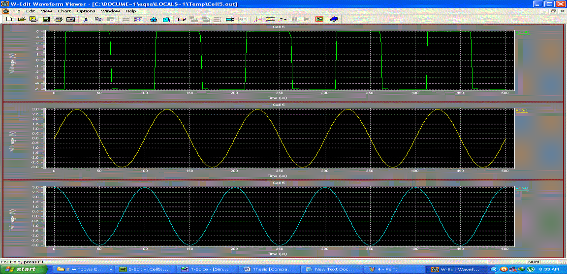
| A comparator generates a logic output high or low based on the comparison of the analog input with a reference voltage. In an ideal comparator, with infinite gain, for input voltages higher than the reference voltage, the comparator outputs logical one and for the input voltages lower than the reference voltage it produces zero at the output. |
| In the below Figure „In-„given to the -ve terminal and the In+ given to the +ve terminal of comparator, when In+ > In- the output is Out (5 volts) and 0 volts when In+ < In-. |
CONCLUSION
|
| A successive approximation ADC is suitable for operation at ultra low supply voltage is realized in a 0.13um CMOS technology using standard threshold CMOS devices and avoiding the bootstrapping techniques. This SAR ADC is well suited for biomedical applications such as Pacemaker, MRI and EEGs. In this paper we mainly focused on designing of low power comparator for SAR ADC in biomedical applications, because comparator in the SAR ADC consumes more power compared to other parts in the SAR ADC. |
Figures at a glance
|
 |
 |
 |
 |
| Figure 1 |
Figure 2 |
Figure 3 |
Figure 4 |
|
 |
 |
 |
 |
| Figure 5 |
Figure 6 |
Figure 7 |
Figure 8 |
|
References
|
- Rudy van de Plassche, “CMOS Integrated Analog-to-Digital and Digital-to-Analog Converters” 2nd Edition, Springer International Edition.
- John F. Wakerly, “Digital Design Principles and Practices”, 3rd Edition, Pearson Education.
- Douglas A.Pucknell& Kamran Eshraghian, “Basic VLSI Design”, 3rd Edition, Prentice Hall of India Pvt.Ltd.
- R.Jacob Baker, Harry W. Li, David E. Boyce, “CMOS Circuit Design, Layout and Simulation”
- Randall L.Geiger, Phillip E.Allen and Noel R.Strader, “VLSI Design Techniques For Analog And Digital Circuits”, McGraw-Hill Inc,1990.
- Hui Zhang, Yajie Qin, Zhiliang Hong. A 1.8-V 770-nW Biopotential Acquisition System for Portable Applications. IEEE Proc. BiomedicalCircuits and Systems Conference, 2009: 93
- Naveen Verma, A.P. Chandrakasan. An Ultra Low Energy 12- bit Rate-Resolution Scalable SAR ADC for Wireless Sensor Nodes. IEEE J.Solid-State Circuits, 2007, 42(6): 1196
|