International Journal of Advanced Research in Electrical, Electronics and Instrumentation Engineering
ISSN ONLINE(2278-8875) PRINT (2320-3765)
ISSN ONLINE(2278-8875) PRINT (2320-3765)
| Riyas T M1, Anusooya S2 |
| Related article at Pubmed, Scholar Google |
Visit for more related articles at International Journal of Advanced Research in Electrical, Electronics and Instrumentation Engineering
A continuous-time low-pass reconfigurable Gm-C filter exhibiting a tuning wide bandwidth is presented. The filter uses a wide frequency, linear operational transconductance amplifier (OTA). The operational transconductance amplifier takes an advantage of common mode feed forward (CMFF), two cross-coupling pairs with source degeneration and cascoding topology to realize a low power multi-band filter performance. Based on the proposed idea, a 1st-order low pass Gm-C filter prototype has been designed in 0.18μm standard CMOS process. Simulated results show the filter is tunable in frequency from about 15KHz to 15MHz. The power consumption of the filter ranges from 9uW to 10mW, and it is operated with 3.3V supply voltage. The cut-off frequency of the filter is tuned by changing the dc bias current of the OTA.
Keywords |
| Gm-C filter, OTA, Common Mode Feed Forward (CMFF), Cascode Topology |
INTRODUCTION |
| Recent trends and developments in portable applications and systems have lead to a significant in wireless standards. Therefore, cost and efficiency of CMOS technology implementation has been tremendously enhanced with the emergence of multi-mode wireless applications. Now multi-mode/multi-band wireless receivers are designed based on the persuasion of reuse [1][4]. Chip designing is the soul of electronic art. Designer should avoid using multiple chipsets and can be made tunable which makes them more efficient in term of area and power consumptions. In a flexible receiver front-end, analog baseband filtering is a key task as it is used to select the required information under desired channel bandwidth. |
| A large tuning range of the analog low-pass filter is widely used in many areas, such as wireless transceivers, channel selection in the system, anti-aliasing and smoothing application [2]. Due to the open-loop operation behavior, Gm-C filter usually use operational transconductance amplifier (OTA) driving a capacitor load at the cost of moderate linearity, sensitivity to parasitic capacitance and high frequency performance. An OTA is a voltage controlled current source (VCCS). The key attractive properties of OTA are their fast speed in relation with conventional low impedance operational amplifiers, and their bias is based on transconductance tunability [6]. Furthermore, the major disadvantage of OTA is the large distortion caused by the nonlinear behavior of the transistors involved. The existing design having high power consumption and low cutoff frequency tuning range, because of the large non-linearity and distortion at the output. This does not provide high impedance at the output and transconductance for the required filter operations. |
| This paper introduces a low power multi-mode Gm-C low pass filter, functionally equivalent to a first order LPF. The proposed circuit designed by the proper combination of common mode feed forward (CMFF), two cross-coupled differential pairs with source degeneration and cascoding the transistors |
| In Section II, the multi-band linear transconductor Gm is presented. The design of the proposed 1st order low-pass filter architecture is given in Section III. Simulated results are described in Section IV. The conclusion is depicted in Section V. |
II. PROPOSED OPERATIONAL TRANSCONDUCTANCE AMPLIFIER (OTA) |
A. Implementation of the Proposed Linearization Transconductor |
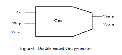
| In order to achieve a good tuning range of the filter, the range of the transconductance should be increased. Usually, Gm-C filter is preferred in high frequency application because of its open-loop operation. The filter performance is largely determined by the Gm value of the OTA. The basic building block in filter design is the integrator which consists of an OTA and a load capacitor [2]. The double ended Gm generator is shown in Figure 1. |
 |
| The proposed OTA circuit consummate on the common mode feed forward (CMFF) and cross-coupling pairs with source degeneration is depicted in Figure 2. The common mode feed forward scheme (NM7, NM9) ideally cancel the harmonic distortion components seem at the output with the same amplitude and phase when the differential output current is processed. The two cross-coupled differential pairs (NM1-NM3, NM2-NM4) at the input level reduce the nonlinearities as designated in the Figure 2. |
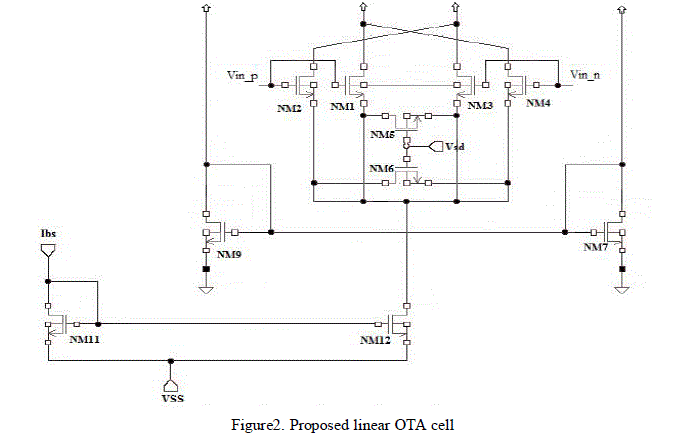 |
| The source degeneration resistors NM5 and NM6 furthermore improve the linear behavior of the OTA structure. The transconductance is restricted by the value of these resistors. The linearity of the transconductor with passive source degeneration resistor cannot be realized perfectly. So the active MOS resistor works in triode region fulfill the requirements [3]. A major advantage of this transconductor is that the quiescent current of the transistor does not vary with the tuning voltage. |
| MOSFET NM11 and NM12 are used for driving the bias current to the OTA in order to tuning the DC transconductance. At the high cut-off frequencies all the transistors operate in the saturation region and at the low frequencies in the weak-invertion region except for the transistors NM5 and NM6. |
 |
| The MOS transistor is approximated the value as |
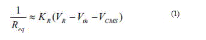 |
| Where KR is relative to MOS process parameter, VR is control voltage of source degeneration resistor, and VCM is common mode voltage of tuning current source. In the Figure2, linearization is realized because the IOUT is expressed as |
 |
| Where gm is the transconductance of MOS transistor. |
| B. The Simulation of the proposed linear Operational Transconductance Amplifier |
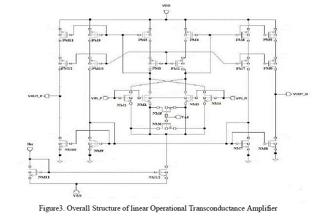
| The overall structure of the linear operational transconductance amplifier (OTA) is shown in Figure 3. The gain bandwidth product (GBW) of the proposed OTA is verified by using 1pF as the loading capacitance. |
| The AC response simulation of the OTA gives the bandwidth of unit gain is about 25MHz, and the phase margin is about 180degree. The Transconductance Gm plot with the input voltage as depicted in the Figure 4. |
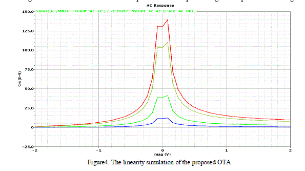 |
| The linear range of the proposed transconductance cell with CMFF and cross-coupling pairs with source degeneration resistance are from -2V to +2V. The transconductance value is ranges from 12nS to 140nS. |
III. THE PROPOSED LOW-PASS FILTER ARCHITECTURE |
| To demonstrate the basic building block in a system level, a first order lo-pass filter prototype is implemented using proposed OTA, as shown in Figure 5. |
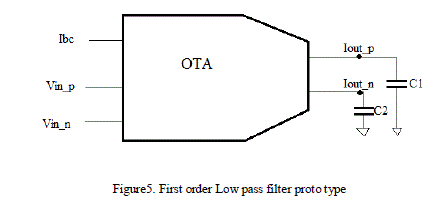 |
| In multi-band low-pass filter design, the cut off frequency of the filter is proportional to gm/C, where gm is the transconductance and C is the capacitance. Here the load capacitors CI and C2 are NMOS capacitors instead of MIM capacitor. The use of NMOS capacitor as load capacitor, it shows the two terminals N-well capacitor operated in accumulation mode exhibits good linearity [2]. |
 |
| In order to operate the NMOS capacitor into accumulation region, the voltage across the capacitor needs to be higher than a reasonable value [2]. The benefit of using NMOS capacitor rather than MIM capacitor is it occupy much less area and also provides decent linearity |
| The cutoff frequency of the Gm-C is tuned by the changing the DC bias current of the operational transconductance. Because, to achieve wide cutoff frequency range the transconductance range should be quite wide. The capacitor value shown in the Figure 5 is 1pf and it is easy to integrate with other sub-circuits. |
IV. RESULTS AND DISCUSSIONS |
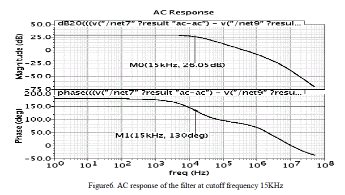
| The frequency and phase response of the filter is given in Figure 6. The AC gain and phase margin of the filter is about 26dB and 140degree, respectively when the cutoff frequency is 15KHz. At this stage of operation all the MOSFETs are in weak- inversion region except source degeneration resistors. The distortion due to the leakage current at this region is ideally eliminated by the common mode feed forward structure of the proposed OTA cell. |
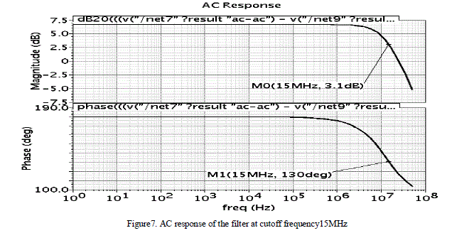 |
| The AC gain and phase margin of the filter is about 3.7dB and 130 degree when the cutoff frequency is about 15MHz as shown in Figure 7. At this stage of operation all the MOSFETs are operated in saturation region except source degeneration MOSFETs |
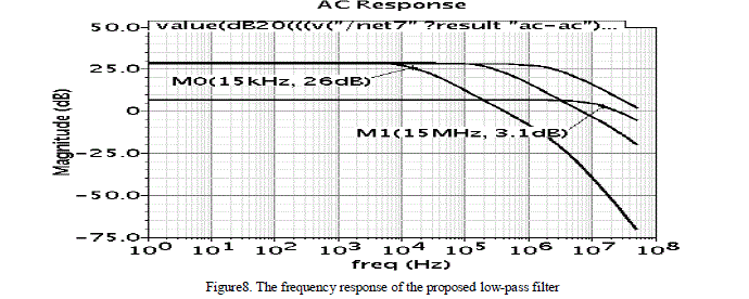 |
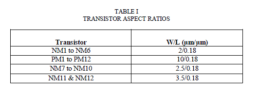
| The low-pass filter cutoff frequency can be tuned about 15KHz to 15MHz as shown in Figure 8.The transconductor was tested with bias current ranges from 40nA to 900uA and the supply voltage of 3.3V. The transistor dimensions are listed in the TABLE I. |
 |
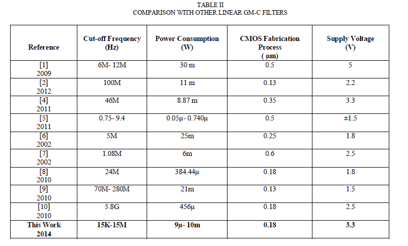
| The comparison result of different existing design of linear Gm-C filter is prescribed in the TABLE II. This shows the proposed design achieved a wide range of cutoff frequency and low power consumption than existing design. Most the recent works are implemented in 180nm CMOS process, in order to reduce the area of the chip. The wide cutoff frequency is obtained, because of high linear and low harmonics in the circuit. The linearity range is about ±2V |
 |
V. CONCLUSION |
| In this paper, Operational Transconductance Amplifier based on CMFF and cross-coupling pairs with source degeneration structure is designed with its transconductance. A first order low-pass filter is designed with the OTAs as the main functional block. Simulated results show the filter achieves cutoff frequency tuning range of 15KHz~ 15MHz in 0.18μm standard CMOS process. It can be used as baseband channel selection of low-pass filter in multi-mode/ multiband receivers |
References |
|