International Journal of Advanced Research in Electrical, Electronics and Instrumentation Engineering
ISSN ONLINE(2278-8875) PRINT (2320-3765)
ISSN ONLINE(2278-8875) PRINT (2320-3765)
Jayachandran.T1, Arulanantham.D1
|
| Related article at Pubmed, Scholar Google |
Visit for more related articles at International Journal of Advanced Research in Electrical, Electronics and Instrumentation Engineering
Comparators play a very important role in high speed analog to digital converters, to maximize speed and power efficiency. In this paper a clocked comparator has been used since can make fast decisions due to the strong positive feedback in the regenerative latch. The accuracy is given by its input referred offset voltage, essential for the resolution of high performance ADC’s. This is methods of reducing power and delay in dynamic latch comparator circuit over the double tail comparator and pre-amplifier based comparators. In order to reduce the circuit delay we are going to use double tail transistor, one at the top Vdd and other at the bottom Vss, by including this transistor positive feedback during regeneration is strengthened, which reduces delay time. In the proposed comparator, power consumption and delay are reduced significantly to 7.4ns and 12 μw respectively. Post-layout simulation results in 0.18-μm CMOS technology used for results analysis.
Keywords |
| conventional dynamic comparator, Analog to Digital Converters, double tail comparator, regenerative comparator. |
I.INTRODUCTION |
| The high speed Analog To Digital Converters (ADC’s) are being has continuously pushed towards their performance limits as technology scales down and system specification become more challenging. In “wearable computing” appliances the ultra-low power consumption requirement originating and also increase the sampling rates in modern communication systems among the rest, make challenge on ADC design. As comparator are most probably second most widely used electronic component after operational amplifier in this era, so it is used in abundance in A/D converters. A comparator is also known as 1 bit analog to digital converter. In analog to digital conversion process, it is necessary to first sample input (using sample and hold circuit) and is applied to a combination of comparators to determine the digital equivalent of the analog signal. The conversion speed of the comparator is controlled by the decision making response time of the comparator. The ultra-deep sub micrometer (UDSM) CMOS technology suffers from low supply voltage especially when considering the fact that threshold voltages of the devices have not been scaled at the same pace as the supply voltage of the modern CMOS process [19]. So designing high speed comparator is more challenging when supply voltage is smaller. So to achieve high speed, large transistor are required to compensate the reduction of supply voltage, which also lead to more die area and power is needed. The low-voltage operation results in limited common mode input range, which is more important for many high speed ADC architectures, such as flash ADC’s. |
| This paper is organized as follows. The section II investigates the operation of conventional dynamic comparator and it’s result. Section III gives the operation and result of double tail comparator. Section IV gives the operation of proposed double tail comparator and its result. Section V presents, list of comparison between different types of comparator. Finally, in section VI some conclusions are drawn. |
II. RELATED WORKS |
| A. Sougata Ghosh, Samraat Sharma[21] presented a novel on “Design of A Novel High Speed Dynamic Comparator with Low Power Dissipation for High Speed ADCs” CMOS dynamic comparator using dual input single output differential amplifier as latch stage suitable for high speed analog-to-digital converters with High Speed, low power dissipation and immune to noise than the previous reported work is proposed. Back to-back inverter in the latch stage is replaced with dual-input single output differential amplifier. |
| V. Narasimha Nayak, Dr. Fazal Noor[22] presented a novel on “High Speed and Low Power Dynamic Latched Comparator for Air Craft Application” a design for an on-chip high-speed dynamic latched comparator for high frequency signal digitization. The dynamic latched comparator consists of two cross coupled inverters comprising a total of 9 MOS transistors. The measured and simulation results show that the dynamic latched comparator design has higher speed, low power dissipation and occupying less active area compared to double tail latched and preamplifier based clocked comparators. |
| Heung Jeon presented a novel on[23] .“Low-power low-offset fully dynamic CMOS latched Comparator” A new fully dynamic latched comparator which shows lower offset voltage and higher load drivability than the conventional dynamic latched comparators has been designed. With two additional inverters inserted between the input and output-stage of the conventional double-tail dynamic comparator, the gain preceding the regenerative latch stage was improved and the complementary version of the output-latch stage, which has bigger output drive current capability at the same area, was implemented |
| Pierluigi Nuzzo, Fernando De Bernardinis[24], Pierangelo presented a novel on “Noise Analysis of Regenerative Comparators for Reconfigurable ADC Architectures” a method to estimate the input referred noise in fully dynamic regenerative comparators leveraging reference architecture. A time-domain analysis is proposed that accounts for the time varying nature of the circuit exploiting some basic results from the solution of stochastic differential equations. The resulting symbolic expressions allow focusing designers’ attention on the most influential noise contributors. |
| Jaeha Kim, Brian S. Leibowitz, and Chris J[25]. Madden presented a novel on “Simulation and Analysis of Random Decision Errors in Clocked Comparators” describes a linear, time-varying (LTV) model of clock comparators that can accurately predict the decision error probability without resorting to more general stochastic system models. |
III. CONVENTIONAL DYNAMIC COMPARATOR |
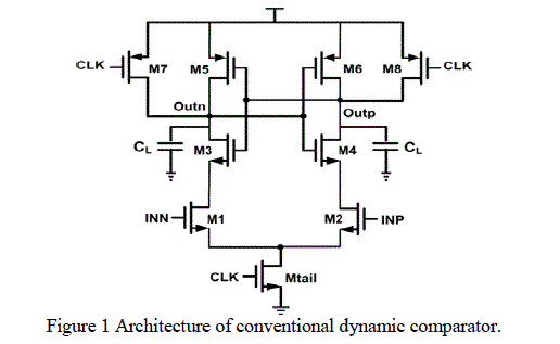 |
| The operation of the comparator is as follows. Start condition will happen when CLK=0(low), which leads to Mtail off and other transistor M7 & M8 makes both the output nodes Outp and Outn to VDD [1]. When CLK=VDD(high), transistor M7 and M8 ear off and Mtail is on. An output voltage which was pre- charged to high voltage, will start to discharge with different rates depending on the corresponding input voltage (INN/INP). |
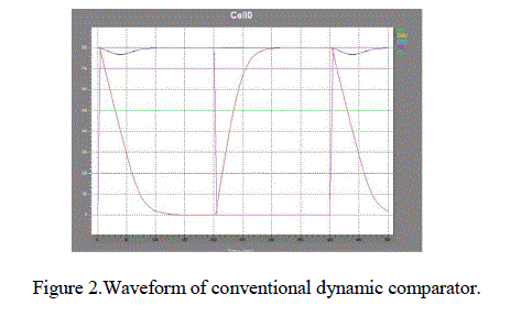 |
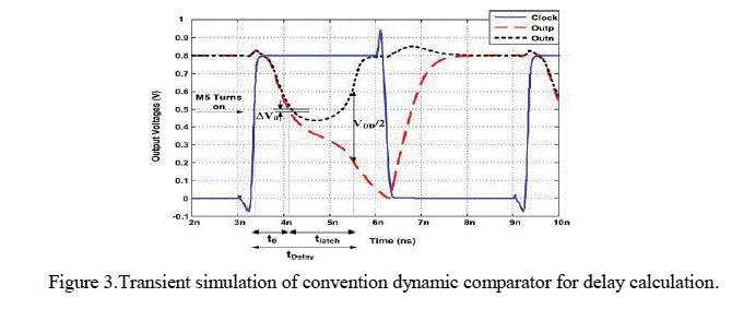
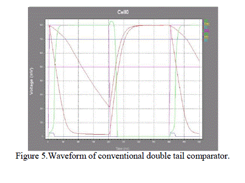
| Assuming the case where VINN > VINP, Outn discharges faster than Outp, hence when Outn (discharged by transistor M1 drain current), falls down to VDD --|Vthn| before Outp (discharged by transistor M2 drain current) the corresponding pMOS transistor (M6) will turn on initiating latch regeneration by inverters(M3, M5 and M4, M6). Thus, Outp pulls to VDD and Outn discharges to ground. If VINN < VINP, the circuit works vice versa. As shown in the figure 2. Figure 3 shows the delay analysis of the conventional dynamic comparator output, from that we can calculate t0 delay, which represent the capacitive discharge of the load capacitance CL until the first P-channel transistor (M5/M6) turns on. And another tlatch delay occur is due to cross coupled inverter. |
 |
| This structure has the advantages of high input impedance [13], rail-to-rail output swing [14], no static power consumption [15]and good robustness against noise [16]. |
IV.DESIGN METHODOLOGY |
| Conventional Double Tail Comparator |
| The systematic diagram of conventional comparator is shown below in figure 4. |
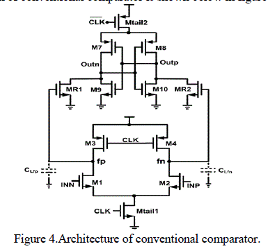 |
| The operation of this comparator is as follows (see Fig. 4) [11]. During reset phase (CLK = 0, Mtail1, and Mtail2 are off), transistors M3-M4 pre-charge fn and fp nodes to VDD, which in turn causes transistors MR1 and MR2 to discharge the output nodes to ground. During decision-making phase (CLK = VDD, Mtail1 and Mtail2 turn on), M3-M4 turn off and voltages at nodes fn and fp start to drop with the rate defined by IMtail1/Cfn(p) and on top of this, an input-dependent differential voltage ΔVfn(p) will build up [10]. |
| Similar to the conventional dynamic comparator, the delay of this comparator comprises two main parts, t0 and tlatch. The delay t0 represents the capacitive charging of the load capacitance CLout (at the latch stage output nodes, Outn and Outp) until the first n-channel transistor (M9/M10) turns on, after which the latch regeneration starts; thus t0 is obtained. |
 |
V. CIRCUIT DESIGN AND TECHNOLOGY CONSIDERATIONS |
| The schematic architecture of proposed comparator is shown below in Figure 6. . The main idea of the proposed comparator is to increase ΔVfn/fp in order to increase the latch regeneration speed. For this purpose, two control transistors (Mc1 and Mc2) have been added to the first stage in parallel to M3/M4 transistors but in a cross-coupled manner The operation of the proposed comparator is as follows (see Fig. 6) [1]. |
| During reset phase (CLK = 0, Mtail1 and Mtail2 are off, avoiding static power), M3 and M4 pulls both fn and fp nodes to VDD, hence transistor Mc1 and Mc2 are cut off. Intermediate stage transistors, MR1 and MR2, reset both latch outputs to ground. |
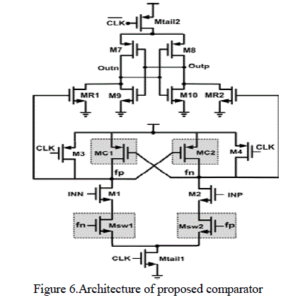 |
| During decision-making phase (CLK = VDD, Mtail1, and Mtail2 are on), transistors M3 and M4 turn off. Furthermore, at the beginning of this phase, the control transistors are still off (since fn and fp are about VDD)[3]. |
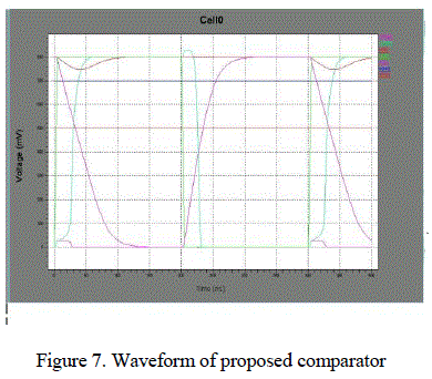 |
| Thus, fn and fp start to drop with different rates according to the input voltages. Suppose VINP > VINN, thus fn drops faster than fp, (since M2 provides more current than M1). The power analysis is shown in the Figure 8. |
VI. RESULTS AND DISCUSSION |
| Thus, fn and fp start to drop with different rates according to the input voltages. Suppose VINP > VINN, thus fn drops faster than fp, (since M2 provides more current than M1). The power analysis is shown in the Figure 8. |
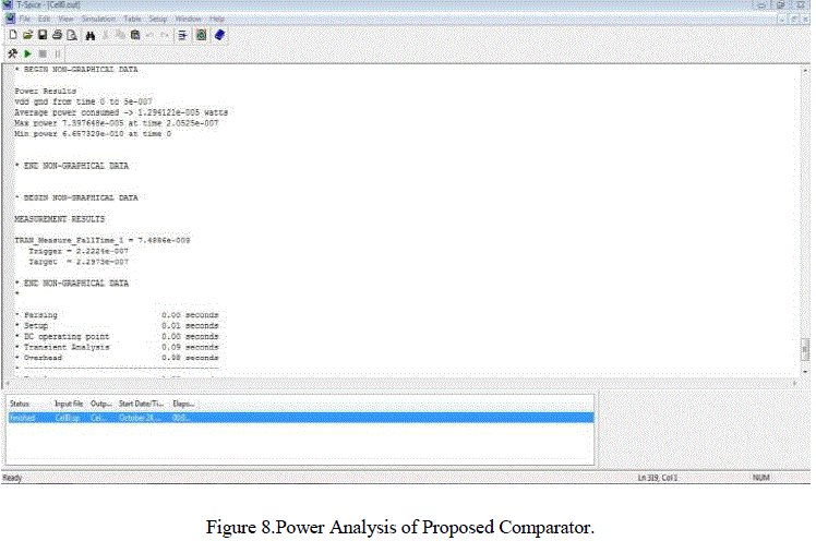 |
| By using the 180-nm technology with supply voltage of 0.8 v we get the delay and power consumption as follows |
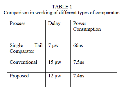 |
| The Table 1 shows that the proposed method reduced the delay from the conventional method. Not only delay but also the power is also reduced significantly from 7.5ns to 7.4ns. |
VII.CONCLUSION |
| Thus two basic structure of comparator where analyzed, based on that a new type of comparator was designed with low power and low voltage, which has improved the performance of comparator. The post layout simulation result in 180nm CMOS technology confirmed that the delay and power consumption of the comparator is reduced to great extent. A two bit flash Analog to Digital Converter can be designed using this type of proposed comparator. |
References |
|