International Journal of Advanced Research in Electrical, Electronics and Instrumentation Engineering
ISSN ONLINE(2278-8875) PRINT (2320-3765)
ISSN ONLINE(2278-8875) PRINT (2320-3765)
Linet. K1, Umarani.P2, T. Ravi2
|
| Related article at Pubmed, Scholar Google |
Visit for more related articles at International Journal of Advanced Research in Electrical, Electronics and Instrumentation Engineering
Designing high speed and low power circuits with CMOS technology have great importance in VLSI circuits. One of the efficient logics among the logic family is the Constant Delay (CD) logic style. In this paper CD logic has been modified and a new logic known as the Low Power High Speed (LP-HS) is proposed. With the help of three changes introduced in the constant delay logic style LP-HS logic is developed which reduces the power delay product. A 4 bit Wallace tree multiplier and Radix 4 multiplier have taken which is then analysed using the constant delay logic as well as LP-HS logic. A comparison has been done on account of the power, delay as well as the power delay product for both the multipliers. The simulations were done using HSPICE tool in 45nm, 32nm, 22nm and 16nm CMOS technologies. The multipliers using LP-HS logic is better in terms of power, delay and power delay product when compared to constant delay logic style.
Keywords |
| CMOS, MOSFET, VLSI, Power Consumption, Delay, Power delay product (PDP), Constant Delay Logic (CD logic). |
I.INTRODUCTION |
| High performance energy efficient logic style is having crucial importance in VLSI circuits. CMOS is the dominant technology which is used to construct these type of integrated circuits. The three most widely accepted parameters to measure the quality of a circuit or to compare various circuit styles are area, delay and power.[2] Advances in CMOS technology have led to improvement in the performance in terms of area, power or delay. There always exists a tradeoff between area, power and delay in a circuit. [14] The power delay product is a figure of merit for comparing logic circuit technologies or families. |
| Constant delay logic style is targeting at high speed applications. The constant delay characteristic of this logic style makes it suitable in implementing complicated logic expressions such as addition. The multipliers play a major role in arithmetic operations. In this paper a Wallace tree multiplier and radix 4 multiplier have taken and is then analysed using both the constant delay logic style as well as Low Power High Speed logic. [4] |
II.RELATED WORK |
| CMOS is the widely used technology to construct integrated circuits. Static CMOS is the most widely used logic style which consists of pull down network (PDN) and pull up network (PUN). It is truly an extension of the static CMOS inverter with multiple inputs. This logic is static because 1 and 0 are restored by pull up and pull down network respectively. This type of design is having high functional reliability and is very easy to design. Requirement of large implementation area is the major disadvantage of this technique. Despite its advantages static CMOS suffers from increased area, and correspondingly increased capacitance and delay. Thus we go for pseudo nMOS logic. It is a ratioed logic. The major advantage of this technique is the low area cost which in turn low input gate load capacitance. The major drawback of this technique is the non-zero static power dissipation. |
| Even though pseudo nMOS logic is having many advantages , because of its static power dissipation we go for dynamic logic. Dynamic logic uses a technique called dynamic precharging. Normally during the time the output is being precharged , the nMOS network should not be conducting. This is usually not possible. Because of the disadvantage of the above logic another type of dynamic logic called the precharge-evaluation logic is proposed. The drawback of this logic is charge lekage, charge sharing and the cascading problem. Monotonicity problem also exists in case of dynamic logic. In order to mitigate the problems of the dynamic logic several modifications for the existing dynamic logic is made which leads to the introduction of CMOS domino logic, self timed domino logic, NORA domino (NP CMOS) etc. Inorder to eliminate the problems associated with the domino logic a new type of logic called feedthrough logic has introduced. Basic feedthrough logic is modified in many ways to get rid of the drawbacks associated with them.To mitigate the problems associated with the feedthrough logic (FTL) a new high performance logic known as constant delay logic style has been designed . This high performance energy efficient logic style has been used to implement complicated logic expressions |
III.CONSTANT DELAY LOGIC STYLE |
| Designers of digital circuits often desire fastest performance. This means that the circuit needs high clock frequency. Due to the continuous demand of increase operating frequency, energy efficient logic style is always important in VLSI. One of the efficient logics which come under CMOS dynamic domino logic is the feedthrough logic (FTL).[3][7][8]Dynamic logic circuits are important as it provides better speed and has lesser transistor requirement when compared to static CMOS logic circuits. Feedthrough logic has low dynamic power consumption and lesser delay when compared to other dynamic logic styles.[9][10][11] |
| To mitigate the problems associated with the feedthrough logic new high performance logic known as constant delay (CD) logic style has been designed. It outperforms other logic styles with better energy efficiency. This high performance energy efficient logic style has been used to implement complicated logic expressions.[1] It exhibits a unique characteristic where the output is pre-evaluated before the input from the preceding stage is ready. Constant delay logic style which is used for high speed applications is shown in Fig 1. |
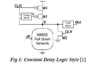 |
| CD logic consists of two extra blocks when compared to feedthrough logic. They are the timing block (TB) as well as the logic block (LB). Timing block consists of self reset technique and window adjustment technique. This enables robust logic operation with lower power consumption and higher speed. Logic block reduces the unwanted glitch and also makes cascading CD logic feasible. The unique characteristic of this logic is that the output is pre-evaluated before the inputs from the preceding stage got ready. An Nmos pull down network is placed where the inputs are given. Based on the logic which is given in the pull down network we will get the corresponding output. A buffer circuit implemented using CD logic is shown below. The expanded diagram for timing block as well as logic block is also shown in the Fig 2 |
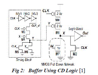 |
| The chain of inverters is acting as the local window technique and the NOR gate as a self reset circuit. Length of the inverter chain varies according to the circuit which we have to design. The prime aim of the inverter chain is to provide a delayed clock. The contention problem which is one of the disadvantages of the feedthrough logic is reduced with the help of this window adjustment. In the self reset circuit one of the input of the NOR gate is the intermediate output node X and the other one is the clock. The logic block is simply a static inverter as in the case of dynamic domino logic. Since the above circuit is for a buffer the NMOS pull down network consists of only one nMOS transistor. |
| The timing diagram for constant delay logic is shown in Fig 3.CD logic works under two modes of operation. |
| i. Predischarge mode (CLK=1) |
| ii. Evaluation mode (CLK=0) |
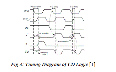 |
| Predischarge mode happens when CLK is high and evaluation mode occurs when CLK is low. During predischarge mode X and Out are predischarged and precharged to GND and VDD respectively. During evaluation mode three different conditions namely contention, C-Q delay and D-Q delay takes place in the CD logic. Contention mode happens when IN=1 for the entire evaluation period. During this time a direct path current flows from pMOS to PDN. X rises to nonzero voltage level and Out experiences a temporary glitch. C-Q delay (clock-out) occurs when IN goes to 0 before CLK transits to low. At this time X rises to logic 1 and Out is discharged to VDD and the delay is measured from CLK to Out. D-Q delay happens when IN goes to 0 after CLK transits to low. During this time X initially enters contention mode and later rises to logic 1 and the delay is measured from IN to Out. |
IV.PROPOSED LP-HS LOGIC |
| The proposed LP-HS logic is derived from the existing constant delay logic. When compared to CD logic there are three major differences in the LP-HS logic. The window adjustment technique is eliminated in this logic. The evaluation transistor is altered as pMOS transistor instead of nMOS. The third variation is the addition of the transistors M2 and M3 in parallel below the pull down network. The proposed logic helps to reduce the power and delay which in turn reduces the power delay product. The circuit diagram for the proposed logic is shown in Fig 4 |
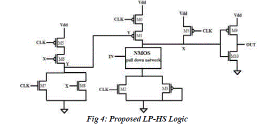 |
| Transistors M0 and M1 whose gates are driven by the CLK and the output of NOR gate are connected in series. This increases the resistance which in turn helps reducing the power. M4 is acting as an evaluation transistor. The NOR gate which is behaving as the self resetting logic is constituted by the transistors M5, M6, M7 and M8. M5, M6 and M7, M8 is driven by CLK and the output intermediate node X. IN values are given to the nMOS pull down network which is given according to the circuit which we have to design. Transistors M2 and M3 are connected in parallel and is placed down to the nMOS pull down network. These transistors help to reduce the power delay product. The gate of M2 is driven by the clock and M3 is at ground. Transistor M2 increases the dynamic resistance of the pull down network which successively helps to reduce the power consumption. Transistors M9 and M10 together figures the static inverter which is used to make the cascading logic more feasible. |
| The circuit works under two modes of operation. |
| i. Precharge mode (CLK=0) |
| ii. Evaluation mode (CLK=1) |
| Precharge mode occurs when clock is low and evaluation mode happens when clock is high. When clock is low, transistor M4 gets ON and provides a high value at node X which in turn provides a low value at the output node OUT. When clock is high the transistor M2 gets ON and the nMOS pull down network is evaluated and gives the output. During this time the transistor M0 whose gate is driven by the CLK is in OFF condition. Due to this the contention mode gets wiped out in the evaluation condition which in turn tends for the elimination of window adjustment technique in the proposed logic. One of the reasons for the power and delay reduction in the circuit is the elimination of the window adjustment technique. During the evaluation mode the pull down network and the transistor M2 gets ON which provides high dynamic resistance which further reduces the power. Transistor M3 is in always ON condition which offers an easy discharge of the value to the ground. |
V.WALLACE TREE MULTIPLIER |
| The multiplier is one of the key hardware blocks in most of the digital and high performance systems such as digital signal processors and microprocessors. Multiplication consists of three steps: partial product generation (PPG), partial product reduction (PPR) and finally carry propagate addition (CPA). Different multiplication algorithms vary in the approaches of PPG, PPR and CPA. |
| The Wallace tree multiplier is considerably faster than a simple array multiplier because of its non linearity. However in addition to the large number of adders required the Wallace trees wiring is less regular and more complicated. As a result, Wallace trees are often avoided by designers, while design complexity is concerned.[12] |
| The Wallace tree multiplier is a high speed multiplier.[5] The summing of the partial product bits in parallel using a tree of carry save adders became generally known as the “Wallace Tree”. Three step process are used to multiply the numbers. |
| Formation of bit products. |
| Reduction of the bit product matrix into a two row matrix by means of a carry save adder. |
| Summation of remaining two rows using a faster ripple carry adder. |
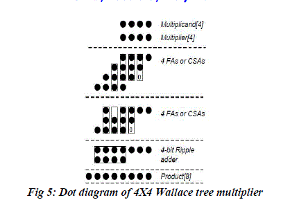
| In the Wallace tree method, three single bit signals are passed to a one bit full adder which is called a three input Wallace Tree circuit, and the output signal (sum) is supplied to the next stage full adder of the same bit, and the carry output signal is therefore passed to the next stage full adder located at a one bit higher position.[13] The dot diagram for a 4x4 Wallace tree multiplier is shown in Figure 2. It describes the dataflow through a 4X4 Wallace tree multiplier in the form of dot diagram indicating the partial product summation at each stage. Each dot represents a ‘0’ or ‘1’. This partial product reduction technique requires 8 CSAs in the first two stages and a 4-bit carry propagate adder at the end.[6] |
 |
| VI. RADIX 4 MULTIPLIER |
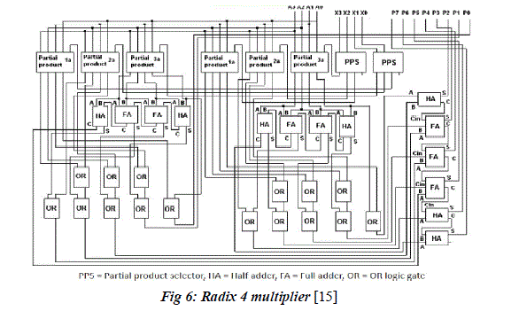
| Addition is an important component of arithmetic operations like subtraction, multiplication and division. Radix 4 multiplier makes use of an adder cell to accomplish the multiplication algorithm.[15] The architecture of a radix 4 multiplier is shown in Figure 6 |
 |
| Basic multiplication can be realized by the shift-add algorithm by generating partial products and adding successive properly shifted partial products. Thus multiplication is proportional to the number of partial products to be added. Radix multiplication algorithms can reduce the number of partial products by handling more than one bit of the multiplier in each cycle. |
| The architecture of the radix 4 multiplier circuit comprises partial product selectors, partial product precomputation blocks, half adder, full adder and OR gate. In the radix 4 multiplier 2 bits per cycle will be considered. From the four bits of the multiplier each two bits are passed to the two partial product selector unit for the further operation. The output generates from the partial product selector is then passed to the six partial product selector units. The generated results from the partial product selector unit is then sent to a set of two half adders and full adders. All the sum values are then passed to a set of OR gate for further calculations. The carry values are passed to the adjacent adders. The two set of eight OR gates generate the two partial products for the next addition. The two generated partial products are again passed to the full adders and half adders for the generation of the output products. The first output bit is directlypassed by one of the partial product precomputation block earlier itself by the AND operation of two bits. |
VII.SIMULATION AND RESULTS |
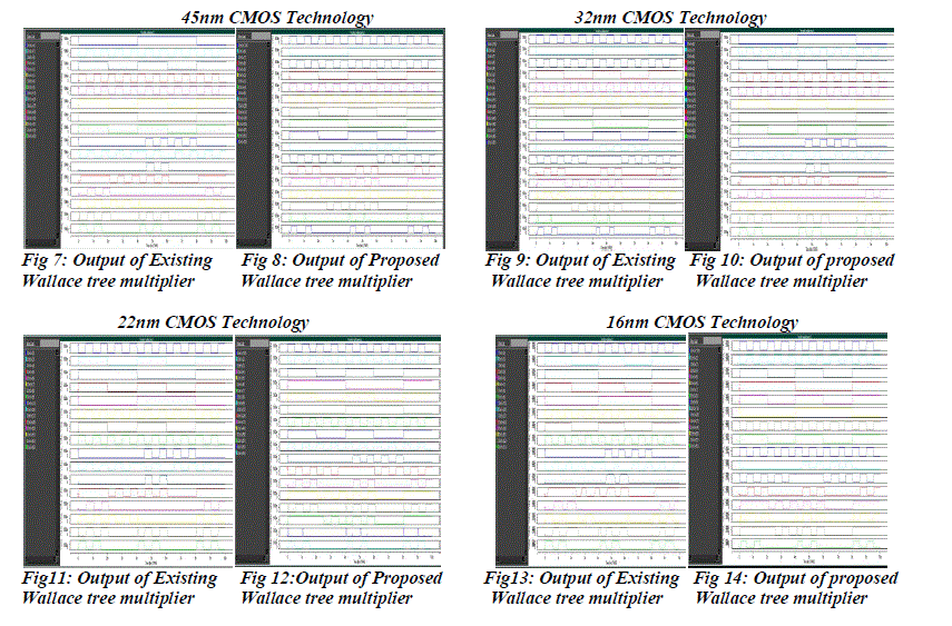
| Figure below shows the output waveform of Wallace tree multiplier using existing logic as well as proposed logic in which V(100) is the clock signal. V(6,7,8,9), V(2,3,4,5) refers the two input signals and the product is represented by V(10,28,37,49,50,51,52,53). |
 |
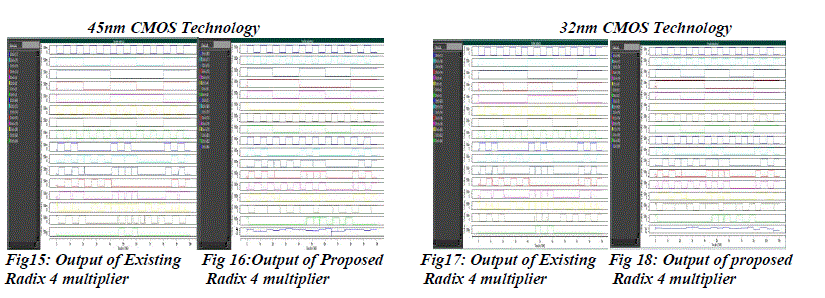
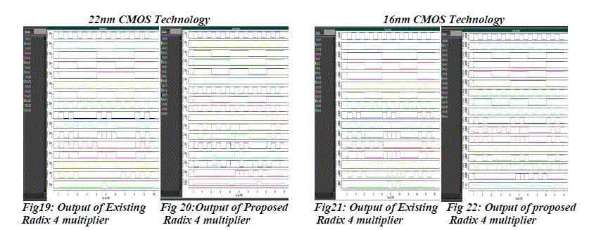
| Figure below shows the output waveform of radix 4 multiplier using existing logic as well as proposed logic in which V(90) is the clock signal. V(14,15,16,17), V(2,3,4,5) refers the two input signals and the product is represented by V(69,70,74,76,78,80,82,84). |
 |
 |
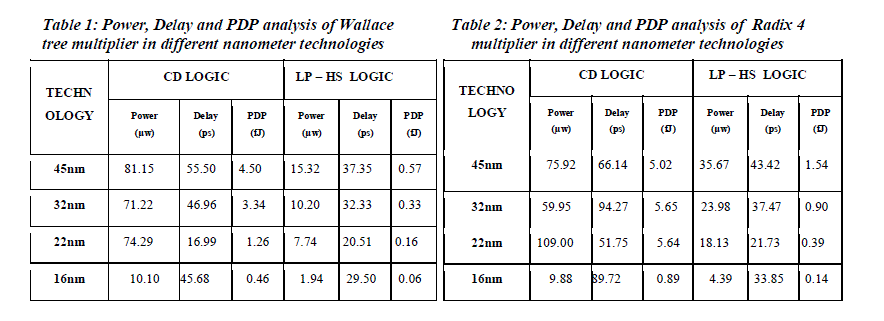
| Here the performance analysis like power, delay and power delay product of Wallace tree multiplier and radix 4 multiplier using CD logic as well as LP-HS logic have been carried out and there results were compared and is shown in the table below. |
 |
VIII.CONCLUSION |
| The concept of constant delay logic is modified and a new logic has been developed known as the LP-HS logic. Multipliers are designed using both existing as well as proposed logic. It is simulated with 45nm, 32nm, 22nm and 16nm CMOS technologies and the performance parameters power, delay, power delay product were compared. The simulations for 45nm, 32nm and 22nm CMOS technologies were carried out at 0.9 V, while 16nm CMOS technology was simulated at 0.6V. The operating frequency for all the technologies was kept at 1GHz. From the results it is found that the power delay product has been improved by 87.33% for Wallace tree multiplier and 69.32% for radix 4 multiplier using the proposed logic in 45nm CMOS technology. A betterment of 90.11% has been found for Wallace tree multiplier and 84.07% for radix 4 multiplier using the proposed logic for 32nm CMOS technology. Similarly an improvement of 87.30% for Wallace tree multiplier and 93.08% for radix 4 multiplier were found using the proposed logic in 22nm CMOS technology. Finally an improvement of 86.95% and 84.26% has been found for Wallace tree multiplier and radix 4 multiplier in 22nm CMOS technology. |
References |
|