International Journal of Advanced Research in Electrical, Electronics and Instrumentation Engineering
ISSN ONLINE(2278-8875) PRINT (2320-3765)
ISSN ONLINE(2278-8875) PRINT (2320-3765)
M.Ramya1, S.Jeevitha2
|
| Related article at Pubmed, Scholar Google |
Visit for more related articles at International Journal of Advanced Research in Electrical, Electronics and Instrumentation Engineering
Power has become a major issue in modern VLSI design. In digital signal processing systems, multiplier plays an important role but also it consumes more power and area. While using BFD multiplier for designing transposed polyphase decimation filter, it has more dynamic power dissipation which is due to the increased switching activity during multiplication and consumes a large circuit area. Also, the number of addition depends on the number of multiplicand bits which cannot be reduced. To overcome these drawbacks, Dadda multiplier is used for better performance as much as compared to existing system.
Keywords |
| Polyphase decimation filter, Dadda Multiplier architecture, Power dissipation, Carrylook ahead adder, speed. |
I. INTRODUCTION |
| In this paper going to describe about FIR filter. Nowadays, Digital Signal Processing (DSP) is used in a wide variety of real-time applications and is playing an important role in the digital revolution. Finite-impulse response (FIR) digital filters are the most fundamental DSP components. FIR filters have the advantage of stability and easy implementation but the large number of filter taps leads to excessive hardware complexity. Power consumption is another important factor in DSP circuits, especially when used in mobile communication systems. With explosive growth in the demand of portable computing and wireless communication systems, power dissipation is becoming an increasing concern. Higher power consumption reduces the battery lifetime of portable devices, affects device reliability, and increases cooling cost. Therefore, low-power methods are necessary for the design of these DSP-based systems. Since finite-impulse response (FIR) filters are critical to most DSP applications, an energy-aware filter design helps significantly in reducing the total power intake of the system. Reduction of hardware complexity directly relates to lower power consumption therefore, several methods have been reported in the literature to reduce computational complexity.A finite impulse response (FIR) filter is a signal processing filter whose impulse response (response to any finite length input) is of finite duration, because it settles to zero in finite time. The impulse response of an Nth-order discrete-time FIR filter lasts for N+1 samples, and then dies to zero. FIR filters can be discrete-time or continuous-time and digital or analog. |
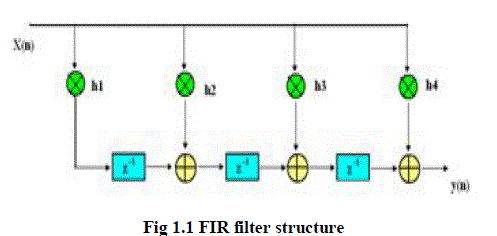 |
| The fig 1.1 shows the FIR filter structure where the input is x(n), h(n) is the coefficients and y(n) is the output. The output y(n) of a linear time invariant system is determined by convoluing its input signal x(n) with its coefficient h(n). For a discrete-time FIR filter, the output is a weighted sum of the current and a finite number of previous values of the input. FIR filter has a number of useful properties which sometimes make it preferable to an infinite impulse response (IIR) filter. They require no feedback. This means that any rounding errors are not compounded by summed iterations. They are inherently stable. This is due to the fact that, because there is no requirement of feedback, all the poles are placed at the origin and thus are located within the unit circle. They can easily be designed to be linear phase by making the coefficient sequence symmetric; linear phase, or phase change proportional to frequency, corresponds to equal delay at all frequencies. This property is sometimes desired for phase-sensitive applications, such as data communications, crossover filters, and mastering. However many digital signal processors provide specialized hardware features to make FIR filters approximately as efficient as IIR for many applications. FIR filters are clearly bounded-input bounded-output (BIBO) stable, since the output is the sum of a finite number of finite multiples of the input values. |
| A multiplier is one of the key hardware blocks in most digital signal processing (DSP) systems. Typical DSP applications where a multiplier plays an important role include digital filtering, digital communications and spectral analysis. Many current DSP applications are targeted at portable, battery-operated systems, so that power dissipation becomes one of the primary design constraints. Since multipliers are rather complex circuits and must typically operate at a high system clock rate, reducing the delay of a multiplier is an essential part of satisfying the overall design. The performance of many computational problems are often dominated by the speed at which a multiplication operation can be executed. Consider two unsigned binary numbers X and Y that are M and N bits wide, respectively. To introduce the multiplication operation, it is useful to express X and Y in the binary. The simplest way to perform a multiplication is to use a single two input adder. For inputs that are M and N bits wide, the multiplication tasks M cycles, using an N-bit adder. This shift-and-add algorithm for multiplication adds together M partial products. Each partial product is generated by multiplying the multiplicand with a bit of the multiplier which, essentially, is an AND operation – and by shifting the result in the basis of the multiplier bit’s position. As a matter of fact, it’s much simpler to perform binary multiplication than decimal multiplication. The entire partial product are generated at the same time and organized in an array. A multi-operand addition is applied to compute the product which is said to be as final. |
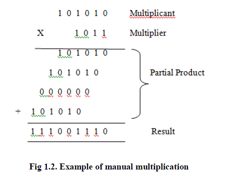 |
| The approach is illustrated in the fig 1.2. This set of operation can be mapped directly into hardware. The resulting structure is called an array multiplier and combines the following three functions: partial-product generation, partial-product accumulation and final addition. |
II. RELATED WORK |
| By reducing the switching activity factor and by minimizing number of operations to be held in the filter structure, the power dissipation can be minimized. Also, the switching activity is reduced by adder and counter [1]. The symmetry or asymmetry property of a linear-phase FIR filter can be exploited to reduce the total number of multipliers into almost half of that in the direct form implementations of the transfer function [2]. A low-power structure is called bypass zero, feed A directly (BZ-FAD) for shift-and-add multiplier architecture which lowers the switching activity in the architecture [3]. For designing the multistage sampling rate conversion FIR filter , Genetic algorithm is used [4]. Systolic decomposition is used for implementing the Efficient FIR filters [5]. For designing the high-speed FIR decimation filters, a bit-level optimized algorithm is used [6]. Here, to design a power aware booth multiplier, an Optimized Wallace tree and pipelining techniques were used [7]. |
| III. EXISTING SYSTEM |
| An FIR filter is characterized by N+1 coefficients of order N and also it require N+1 multipliers and N two-input adders. Some of the filter structures are given below: |
| 3.1 TRANSPOSED POLYPHASE DECIMATION FILTER |
| In this filter, the decimator with a decimation factor D, where D is a positive integer develops an output sequence y(n) with a sampling rate is (1/D)th of the input sequence x(n). Polyphase is a method of doing sampling rate conversion that leads to very efficient implementation. This is implemented by keeping every Dth sample of the input sequence and removing D-1 samples between consecutive samples. As a result, all input samples with indices equal to an integer multiple of D are retained at the output and all others are removed, to produce the output sequence, the following relation is used, |
| Aliasing occurs during decimation, to overcome the aliasing effect ant aliasing filter is used before down sampling called low pass filter. The transposed form of the decimation filter is used in this tapped delay structure to avoid the shift registers used here. Recently, an efficient parallel FIR filter implementation technique requiring a less-than linear increase in the hardware cost was proposed. The architecture involves multiplying all coefficients with the same input data. The circuit is faster because the registers are between the adder blocks reducing the critical path. For that first the filter H(z) should be decomposed to polyphase components. Decimation reduces the sampling rate at the output of a system so that another system can receive this signal as input with a lower sampling rate. By exploiting the constraints on the coefficient values, this architecture yields extremely efficient and high speed programmable and custom implementations. |
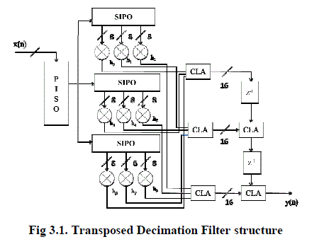 |
| The structure of transposed form of polyphase filter for decimation factor of three is shown in fig.3.1. In this structure, during each cycle, input x(n) is passed through the tap mulitplier. Intially the input sequence x(n) is given through a parallel input serial output (PISO) shift register. The output from PISO is given to three subfilter section where the input sequences are processed in parallel form by means of serial input parallel output (SIPO) shift register. |
| Each section, the input is multiplied with the coefficients. Since the processing is done in parallel, this structure improves the speed of operation. The coefficients are cycled through their values at the sample rate, but the indexes of the coefficients at any given time are separated by D, the decimation rate. The coefficient is multiplied with the sample, but the input samples and coefficients changing during each cycle. The function of the accumulator is to accumulate the value of multiplier for every 3(D) cycles. In order to increase the speed of operation, Carry lookahead adder is used to perform addition. The decimated output y(n) is obtained using this polyphase structure. |
3.2 BFD MULTIPLIER |
| In this multiplier, the switching activity should be reduced to reduce dynamic power dissipation. The switching activity is reduced by replacing some of the components and adding a bypass and feeder logic. Fig.3.5. shows the architecture of BFD multiplier where X and Y are the inputs. In the conventional shift and add multiplier X and Y are the two inputs and to generate the partial product, Y (0) is used to decide between X and 0. If Y(0)=1 then X has to be added to the previous partial product, whereas if it is Y(0)=0, no addition operation is requires to generate the partial product terms. |
| Hence, in each cycle, register Y must be shifted to the 111 right so that its right bit appears at Y(0); this operation leads to some switching activity. To eradicate this problem, in this BFD multiplier architecture, a multiplexer with one-hot encoded bus selector is used in each cycle. Counter is used to select Y(n) in the nth cycle. |
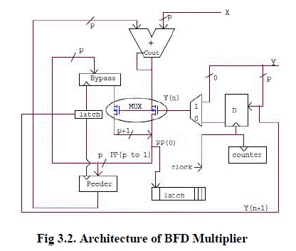 |
| The fig 3.2 shows that in conventional shift and add multiplier, at each cycle, the current partial product is added to X (when Y(0) is one) or to 0 (when Y(0) is zero). This gives rise to unnecessary transitions in the adder when Y(0) is zero. In this BFD multiplier architecture, the adder can be bypassed and the partial product should be shifted to the right by one bit. This minimizes unnecessary switching activities in the adder. In each cycle, the hot bit of the next cycle (Y(n+1)) is checked. If Y(n+1)= 0, i.e., the adder is not required for the next clock cycle, to store the current partial product, the bypass register is clocked. If Y(n+1) is 1, i.e., the adder is really required for the next cycle, to store the current partial product, the feeder register is clocked and this result should be fed to the adder in the next clock cycle. |
IV. PROPOSED SYSTEM |
| Polyphase decimation filter is designed using Dadda multiplier, which reduces the area and power. CLA(Carry Lookahead adder) for improving the speed. The Dadda multiplier is a hardware multiplier design invented by computer scientist Luigi Dadda in 1965. It is similar to the Wallace multiplier, but it is slightly faster (for all operand sizes) and requires fewer gates(for all but the smallest operand sizes).Dadda multipliers have the following three steps: |
| Multiply (logical AND) each bit of one of the arguments, by each bit of the other, yielding results. Depending on position of the multiplied bits, the wires carry different weights, for example wire of bit carrying result of is 32. |
| Reduce the number of partial products to two layers of full and half adders. |
| Group the wires in two numbers, and add them with a conventional adder. |
| A parallel tree multiplier design usually consists of three major steps: |
| PP generation |
| PP reduction, and |
| final carry propagate addition |
| PP generation produces PP bits from the multiplicand and the multiplier. The goal of PP reduction is to compress the number of PPs to two, which is to be summed up by the final addition. The most famous reduction methods are Dadda tree reductions. |
| The Dadda reduction only performs compression whenever Necessary without increasing the number of carry-select addition (CSA) levels, a new reduced area (RA) reduction method was proposed so that the bit width of the final carry propagate adder (CPA) is minimized. |
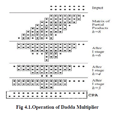 |
| The operation of Dadda multiplier is shown in fig.4.1. It describes how it generates the partial products with its sum and carry in the above stages. To allow for more flexible column-by-column reduction to be used in the proposed truncated multiplier design, we present two reduction schemes that intend to minimize the use of half adders (HAs) in each column because the full adder (FA) cell has a higher compression rate compared with the HA cell. A new reduced area (RA) reduction method was proposed so that the bit width of the final carry propagate adder (CPA) is minimized. |
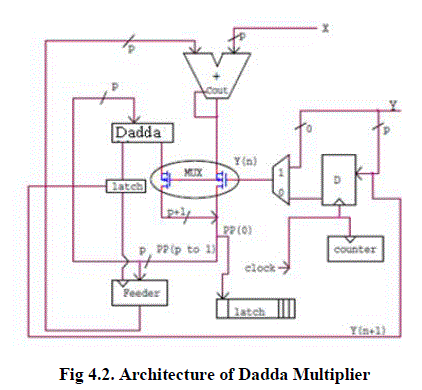 |
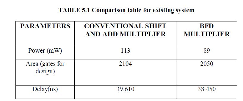
| The fig 4.2 shows that while using Dadda multiplier, delay can be reduced as compared to BFD multiplier. Also, it consumes less power and high area efficient. The proposed design has the following applications such as high speed signal processing that includes DSP based applications, DWT and DCT transforms used for image and wide signal processing, FIR and IIR Filters for high speed, low power filtering applications, multirate signal processing applications such as digital down converters and up converters. |
V. RESULTS AND DISCUSSION |
| The polyphase decimation filter is designed and verified using Xilinx and ModelSim Altera 6.5e. The power dissipation is calculated using Quartus- II 10.0 software.. The results the output of the multiplier which is 16 bits wide. It includes bypass register, feeder register, latches, flip flop, multiplexer, adder and ring counter. The inputs to the filter are clock and reset .The input data and coefficient of filters are stored in registers. It contains BFD multiplier, 16 bit adder and accumulator for storing intermediate results. |
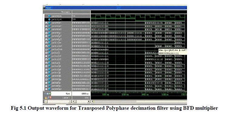 |
| The fig 5.1 shows that the waveform for BFD multiplier which is verified by using verification tool ModelSim 6.3f. It is clearly shown that the output appeared is verified successfully. After that,the waveform is genaerated for input, output and the signal paths. Finally, the 16-bit output is appeared with reset and shift operating conditions. |
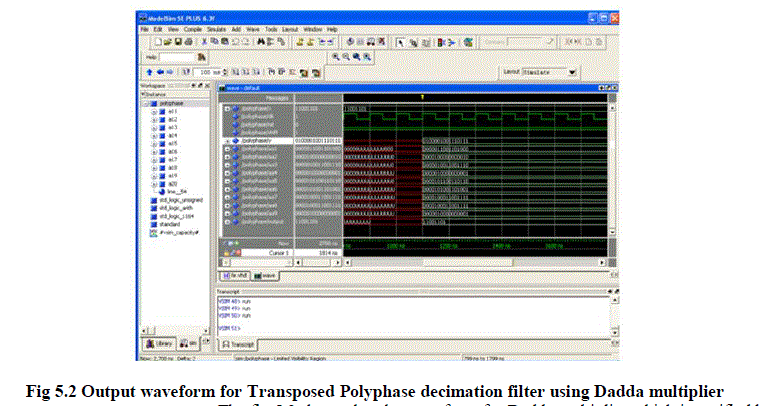 |
| The fig 5.2 shows that the waveform for Dadda multiplier which is verified by using verification tool ModelSim 6.3f. It is clearly shown that the output appeared is verified successfully. After that,the waveform is generated for input, output and the signal paths. Finally, the 16-bit output is appeared with reset and shift operating conditions. |
 |
VI. CONCLUSION |
| The conventional shift and add multiplier occupies more area and also consumes more power. By using the Dadda multiplier in the proposed design, power and area can be reduced when compared to conventional shift and add multiplier. This design also reduces delay as compared to BFD multiplier. |
References |
|