Keywords
|
| CIC Filter, Multirate, Model sim, FPGA. |
INTRODUCTION
|
| Systems dealing with different kind of sampling rates are termed as multirate system. As the need of data conversion is increasing day by day, extraction of narrow band from the wide band sources, and design of narrow band filters with wideband signals are becoming decisive. FPGA used for developing digital signal processing. The large hierarchy of programmable logic blocks within the FPGA gives great re-configurability together with speed. Once programmed, the FPGA may not provide the flexibility of a processor but offers better speed, which is required for many DSP applications In signal processing, most currently used procedure is to adjust sample rate frequency with respect to signal of interest. |
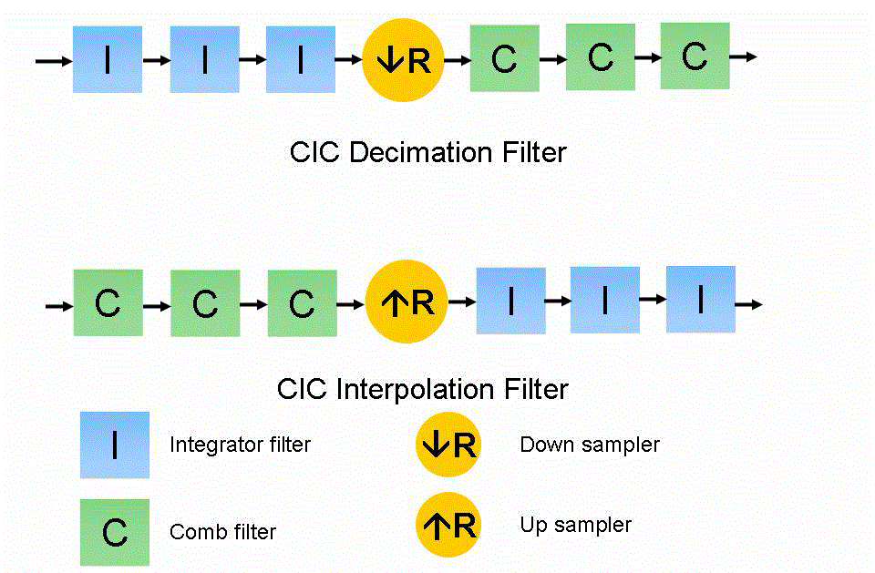
| CIC filter is formed by cascade of digital accumulator (integrator) subsequently chased by a cascade of digital differentiators (combs) in equal Number of stages. Decimator is service to lower the sampling frequency of the comb signals with respect to the system sampling frequency. This is placed in between the multi rate filters. So that CIC filter architecture is enhancement. |
| Consider for Decimation, one can get down computational complexity of narrowband low pass filter as compared with using a single stage FIR, along which the filter operate at reduce clock rates, low power and high speed used CIC filters. It happens of multirate filter more popular, and also designs on architecture that basically uses only without multipliers. |
RELATED WORK
|
| This approach can be applied profitably to Decimator and Interpolator designs, the essential function of Decimation or Interpolation filter is to decrease or increase the sampling rate and to keep the pass band aliasing or imaging error within prescribed bounds. The filters require no multipliers and use limited storage thereby leading to more economical hardware implementations. They are designated cascaded integrator-comb (CIC) filters because their structure consists of an integrator section operating at the high sampling rate and a comb section operating at the low sampling rate. |
| Using CIC filters, the amount of pass band aliasing or imaging error can be brought within prescribed bounds by increasing the number of stages in the filter. However, the width of the pass band and the frequency characteristics outside the pass band are severely limited [1]. |
| The fact that the CIC filters need to operate at such high rates makes their multiplier less-nature attractive for hardware implementation. The CIC up sampling filters usually consist series of single stages rearranged in such a way that all the down sampling filters are grouped together with all the integrator filters. By looking closely at a single-stage CIC interpolator, it has shown a simple trick to reduce the complexity of a multistage implementation. Because multistage CIC interpolators have a single-stage CIC interpolator at its core, this trick will simplify the complexity of any CIC Interpolator [2]. |
| The Cascaded Integrator Comb (CIC) filter is a digital filter which is employed for multiplier-less realization. This type of filter has extensive applications in low-cost implementation of interpolators and decimators. However, there is a problem of pass-band droop, which can be eliminated using compensation techniques. The Farrow filters is another class of digital filters which are used extensively in arbitrary sample rate conversions and fractionally delaying the samples. They have poly-phase structure and are very efficient for digital filtering. |
| In addition to this, Field-Programmable gate Array (FPGA) has become an extremely cost-effective means of off-loading computationally intensive digital signal processing algorithms to improve overall system performance.Sample Rate Converter, CIC filter with and without compensation technique are implemented on, FPGA. Farrow filters are also implemented for fractional delay and arbitrary change in sample rate conversion. |
| Both of these filter configurations provide a better performance than the common filter structures in terms of speed of operation, cost, and power consumption in real-time. The CIC filter is a multiplier free filter that can handle large rate changes. It was proposed by Eugene Hogenauer in 1981 [1]. It is formed by integrating basic 1-bit integrators and 1-bit differentiators. It uses limited storage as it can be constructed using just adders and delay elements. That’s why it is also well suited for FPGA and ASIC implementation. The CIC filter can also be implemented very efficiently in hardware due to its symmetric structure. The CIC filter is a combination of digital integrator and digital differentiator stages, which can perform the operation of digital low pass filtering and decimation at the same time.[3] |
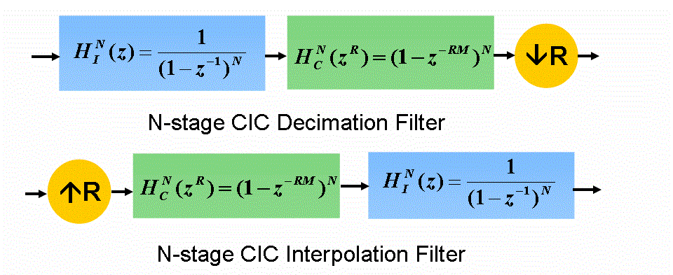
| An integrator filter is a single pole accumulator with a transfer function |
| HI (z) (Equation 1): |
 (1) (1) |
| A comb filter is a differentiator with a transfer function |
 (2) (2) |
| In this equation, M is the differential delay, and is usually limited to 1 or 2. In a CIC filter, the integrators operate at high sampling frequency (fS), and the comb filters operate at low frequency (fS/R). Using the Noble identities, the equivalent frequency response of their cascade can be |
| calculated (Fig 2). |
| Equation 3 shows the total response of a CIC filter at high frequency (fS): |
 (3) (3) |
| In this equation, N is the number of integrator-comb filter pairs, and R is the rate change factor. Equation 3 implies that the equivalent time domain impulse response of a CIC filter can be viewed as a cascade of N rectangular pulses. Each rectangular pulse has RM taps.[3] |
Multi rate filters:
|
| The efficiency of multi rate filters is greatly improved by simplifying arithmetic operations. This is achieved by replacing a multiplier with a small number of shifters-and-adders. Generally, implementing multiplier less design techniques in sub-filters, at the cost of a slight derogation of filtering performances, increases the efficiency of the overall multirate filter. A well-known solution for large conversion factors in decimation is a cascaded integrated comb (CIC) filter, which performs multiplier less filtering [4]. |
PROPOSED WORK
|
Block diagram:
|
| Interpolator: |
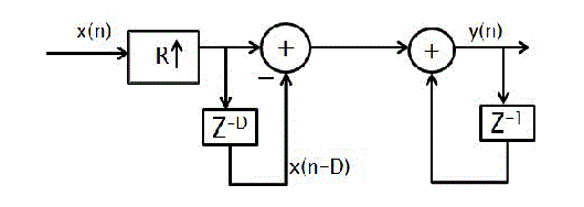
| Up sampling by a factor R is the process of inserting R-1 zero valued samples between original samples in order to increase the sampling rate. The output sample rate increases by a factor R. Upsampling by R adds to the original signal R-1 undesired spectral images which are centered at multiples of the original sampling rate.CIC filters are used as antiimaging filters for interpolated signals in order to remove the unwanted spectral images .The comb section precedes the integrator in a CIC interpolator. Fig 3 depicts the CIC interpolator structure. |
| X(n) is given as sampling rate input, Y(n) is reduced sampling rate output, R is a rate change of factors, Here design on CIC Decimator filer for multi stage series are connected in integrator and comb. Integrator output follows depending on output to Decimator stage with following Decimator delay, so that Decimator output going to CIC output. Optimized design of the number of stages and the choice of decimation factor for the individual stages results in reduction decimation filter. |
| Each integrator contributes to the CIC transfer function with a input. Each comb section contributes with a zero of order D, where D is the frequency decimation ratio. This filter is most often used in signal processing; mainly because of its simplicity and optimal behaviour for common ask like random noise reduction while retaining sharp step response. This makes it a prime filter for time domain encoded signal. At the same time it is worst filter for frequency domain encoded signals with less capacity to separate one band of frequencies from another. |
IMPLEMENTATION AND RESULTS
|
INTERPOLATOR:
|
| RTL verification: |
| 1. Select the interpolator source file in the Source. |
| 2. Open the Design Summary by double-clicking the View Design Summary process in the Processes tab. |
| 3. Double-click the Implement Design process in the Processes tab. |
| 4. Notice that after Implementation is complete, the Implementation processes have a green check mark next to them indicating that they completed successfully without Errors or Warnings as shown in fig 7. |
| The RTL Verilog is then simulated to validate the functionality against the specification. RTL simulation is usually one or two orders of magnitude faster than gate level simulation, and experience has shown that this speed-up is best exploited by doing more simulation, not spending less time on simulation. In practice it is common to spend 70- 80% of the design cycle writing and simulating Verilog at and above the register transfer level, and 20-30% of the time synthesizing and verifying the gates. |
| Simulation Results: |
| • From the above results it can be seen that all the results are triggered at positive edge of clock pulse. when neg edge reset=’0’, all the outputs are zeros. |
| • When neg edge reset = 1. If 8 bit valued counter from ‘00000000’ to ‘00000011’ then count increments up to three clock phase, counter increments by one, integrator operation performed. Whenever counter is equal to ‘00000’this cycle decimator operation preformed. Positive edge pulse rdy operation is done. Finally decimator output goes to CIC filter output performed. |
| • The simulated results are obtained as per requirements. The intermediate results are obtained using pre simulation and post simulation. Some of the simulation results of the decimator are shown in the following figures. |
RESULTS:
|
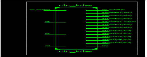
| Device utilization summary for interpolator Number of stages = 5, down sampling rate = 3. And Differential delay = 2 ns |
CONCLUSION
|
| This paper contents related work for CIC interpolator is studied and planned for the circuit design. Here only design only number stage increased and fixed rate change of factor in simulation results. The decimator code (40 bit) is written in verilog format and its RTL Register Transfer Logic architecture is obtained by synthesis of the code. During simulation of the code the wave forms are obtained, CIC filters can implement decimation efficiently in hardware for a wide range of rate change factors. The multirate filtering techniques are widely used in sampling rate conversion systems and constructing filters with equal input and output sampling rates. By using the multistage approach, the total number of coefficients is significantly reduced. |
Figures at a glance
|
 |
 |
 |
 |
| Figure 1 |
Figure 2 |
Figure 3 |
Figure 4 |
|
 |
 |
 |
 |
| Figure 5 |
Figure 6 |
Figure 7 |
Figure 8 |
|
References
|
- Eugene B. Hogenauer, "An Economical Class of Digital Filters for Decimation and Interpolation," IEEE Transactions on Acoustics, Speech, and Signal Processing, vol. ASSP-29, no. 2, pp. 155-162, Apr. 1981.
- P. P. Vaidyanathan and Sanjit K. Mitra.Polyphase Networks, Block Digital Filtering, LPTV Systems, and Alias- Free QMF Banks: A Unified Approach Based on Pseudocirculants. IEEE Transactions on Acoustics, Speech, and Signal Processing, 36(3):381–391, March 1988
- Ricardo A. Losada and Richard Lyons,”Reducing CIC Filter Complexity”,IEEE Signal Processing magazine,pp. 124-126,July 2006.
- Ricardo A. losada,”digital filters with matlab” ,the mathworksinc. ,may 2008 Fredric J. Harris, Multirate Signal Processing for Communicating Systems, 2004
- Charanjitsingh University College, Punjabi university Patiala, India International Journal of Advanced Computer Science and Applications, Vol. 1, No. 6, December 2011.
- B.A.Shenoi,”Introduction to Digital Signal Processing and FilterDesign”,JohnWiley and sons,Inc.,NewJersey,2006
- Uwe Meyer-Baese. “Digital Signal Processing with Field Programmable Gate Arrays”. Springer-Verlag, New York, Inc., Secaucus, NJ, USA, pp. 70-75, 2008.
- J. Mitola, "The Software Radio Architecture," IEEE Communications magazine, vol. 33, no. 5, pp. 26-38, May 1995.
- Ramesh Bhakthavatchalu, Karthika V.S.,Lekshmi”Design and Implementation of Improved Attenuation CIC Decimator and Interpolator in FPGA” International Journal of Recent trends in Engineering and Technology, ACEEE, pg. 18-22, Vol. 6, No.2, Nov2011.
- Rajesh Mehra and ShailyVerma International Journal of Recent Technology and Engineering (IJRTE) ISSN: 2277-3878, Volume-1, Issue-6, January 2013
|