International Journal of Advanced Research in Electrical, Electronics and Instrumentation Engineering
ISSN ONLINE(2278-8875) PRINT (2320-3765)
ISSN ONLINE(2278-8875) PRINT (2320-3765)
| M. I. Ahmed*, 1, E. A. Abdallah1, H. M. Elhennawy2 |
| Related article at Pubmed, Scholar Google |
Visit for more related articles at International Journal of Advanced Research in Electrical, Electronics and Instrumentation Engineering
A compact dumbbell shaped defected ground structure (DGS) is applied to reduce the mutual coupling between microstrip arrays elements for ISM band and wireless applications with 0.47 λ0 elements spacing. The dumbbell DGS with new distribution is inserted in the E-plane between the adjacent arrayscoupled elements to suppress the pronounced surface waves. A four-element array with dumbbell shaped DGS is designed, fabricated on a substrate with dielectric constant of 10.2 and thickness of 1.27mm, and measured. The results show that a reduction in mutual coupling of 35.6 dB is obtained between elements at the operation frequency of the array. The surface current distribution with and Without DGS for the array is discussed. The microstrip array with and without DGS are studied by the waveguide simulator method and fabricated by photolithographic technique.
Keywords |
| Defected Ground Structure, ISM Band, Microstrip Antenna Array, Mutual Coupling |
INTRODUCTION |
| The rapid expansion of wireless technology during the last years has drawn new demands on integrated components including also antennas. The existence of an immense infrastructure worldwide for the 2.4 GHz Industrial, Scientific and Medical (ISM) band along with the release of the 5.6 GHz ISM band, combined with its increasing popularity, related to the Bluetooth and/or WLAN systems applications |
| In this paper, a compact dumbbell shaped defected ground structure (DGS) is applied to reduce the mutual coupling between array elements and reduce the array elements spacing to 0.47 λ0. The dumbbell DGS is inserted between the adjacent E-plane coupled elements in the array to suppress the pronounced surface waves. A linear and planar fourelement array with and without dumbbell shaped DGS are studied. The results show that a reduction in mutual coupling of 35.6 dB is obtained between elements at the operation frequency of the array. |
II. LITEARTURE SURVEY |
| In the late 1990s, defected ground structure (DGS) was firstly proposed by Korean scholar J. I. Park et al. [1]. It is based on the idea of photonic band-gap structure, and applied to the design of planar circuits. DGS is an etched periodic or non-periodic cascaded configuration defect in ground of a planar transmission line [2] (e.gmicrostrip, coplanar and conductor backed coplanar wave guide), which disturbs the shield current distribution in the ground plane. This disturbance will change characteristics of a transmission line such as the line capacitance and inductance to obtain the slow-wave effect and band-stop property [3-6]. Controlling higher order modes up to third harmonic of the fundamental operating frequency in a microstrip line-fed patch antenna [7]. Antenna miniaturization was achieved by loading the patches with complementary split ring resonator (CSRR) [8]. Improving polarization purity (co- to crosspolarized isolation) in probe fed rectangular microstrip patches [9, 10]. There are two main methods for the design and analysis of DGS [11]: the commercially EM software which is the main simulates software to design and analyze DGS, and the equivalent circuit method. |
III. SINGLE ELEMENT |
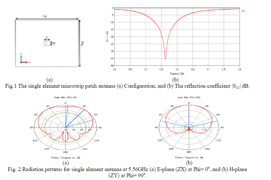
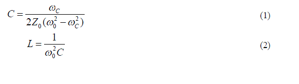
| CST numerical simulator was used to simulate the single microstrip patch antenna on a dielectric substrate with εr = 10.2, h = 1.27 mm, and tan δ = 0.0035. To obtain the resonant frequency at 5.562GHz, the patch size was 7.5 mm x 6 mm. The ground plane is 80 mm x 60 mm (1.48λ0 x 1.1λ0) at resonant frequency to avoid fringing effect as shown in Fig. 1.a. The patch is fed by a coaxial probe feed technique. The simulated reflection coefficient |S11| is presented in Fig. 1.b. The bandwidth of 1.3 % is obtained. The E- and H-plane radiation patterns are shown in Fig. 2. |
 |
IV. TWO ELEMENTS ARRAY |
| The E-plane coupled microstrip patch antenna arrays suffer from strong mutual coupling because of surface waves. Due to the capability of DGS to suppress surface waves, a single dumbbell shape DGS was inserted between two antenna elements in order to reduce the mutual coupling. DGS unit can be modeled by a parallel R, L, and C resonant circuit connected to transmission liens at its both sides as shown in Fig. 3. The equivalent circuit parameters L, C, R of dumbbell- shaped DGS unit can be given by [1]: |
 |
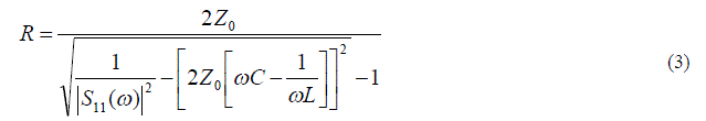 |
| where, ω0 is the angular resonance frequency, ωC is the 3-dB cutoff angular frequency, and Z0is the characteristic impedance of the microstrip line, S11(ω) is the input reflection coefficient of the equivalent circuit network. |
| The LCR equivalent circuit parameters for DGS are given as follows: 1) The resonant frequency ω0, the cut-off frequency ωC and the terminal impedance Z0are obtained by frequency response curves; 2) Calculate the equivalent capacitance C and equivalent inductance L by Equations (1) and (2); and 3) Calculate R by Equations (3). |
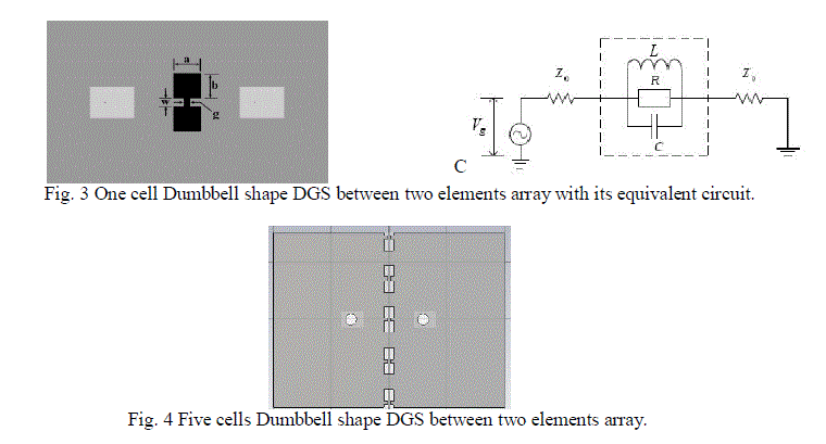
| The mutual coupling can be decreased more by increasing the DGS unit to five cells of dumbbell shape as shown in Fig. 4. CST numerical simulation was used to simulate the E-plane coupled microstrip antennas on a dielectric substrate with εr = 10.2 and h = 1.27 mm. To obtain the resonant frequency at 5.64 GHz, the rectangular patch’s size was 7.375 mm x 6 mm, and to avoid the grating lobes, the distance between the patches was 25 mm (0.47λ0). The defected ground plane is 80 mm x 60 mm (1.5λ0 x 1.2λ0) at resonant frequency to avoid fringing effect. Each patch is TM10 mode excited by a matched coaxial feed 0.7375 mm away from the patch center. The optimum values of the structural parameters of the dumbbell shape DGS are the dumbbell head (a) = 3.6 mm, b = 4 mm, slot length between the dumbbell (w) = 1.24 mm, and slot width (g) = 0.85 mm. |
 |
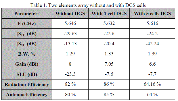
| The simulated mutual coupling |S21| and reflection coefficient |S11| in both cases (i.e., with and without DGS) as shown in Fig. 5 are compared in Table 1. It is observed that DGS antenna resonant frequency shifts downward with respect to the conventional antenna. This small frequency shift is due to slow-wave effects of DGS. The conventional antenna shows a very strong coupling of -15.13 dB due to surface waves pronounced in thick, high permittivity substrate. Since the resonant frequency of the antenna falls inside the DGS band gap, surface waves are suppressed and simulations show that mutual coupling drops to -42.24 dB which is 27.11 dB lower than the conventional one, but with reduction in gain and efficiency as shown in Table 1. |
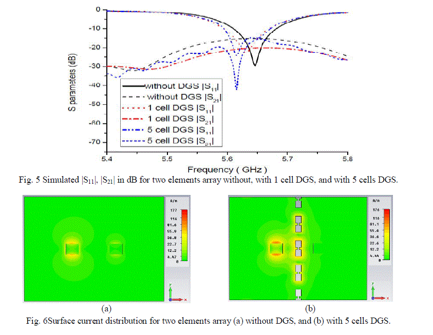 |
| The mitigation of the space-wave by virtue of the DGS structure is clearly observed in Fig. 6, in which the distribution of the surface currents on the ground plane are plotted when one patch antenna is excited while the other patch antenna is terminated with a 50 Ω impedance load. It is clearly seen that without the DGS, the terminated fed patch is strongly excited while with the presence of the DGS, it is very weakly excited. The proposed 5 cells DGS configuration ensures the suppression of the vertically polarized electric fields (space-wave) between the two patches. |
 |
 |
 |
V. LINEAR FOUR ELEMENT ARRAYS |
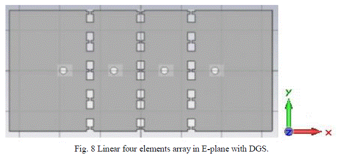
| As shown in Fig. 8, the four elements microstrip patch antennas on a dielectric substrate with εr = 10.2, h = 1.27 mm, and tan δ = 0.0035. The distance between the patches is 25 mm (0.47λ0). The defected ground plane is 130 mm x 60 mm (2.4λ0 x 1.2λ0) at resonant frequency. Each patch is TM10 mode excited by a matched coaxial feed 0.7375 mm away from the patch center |
 |
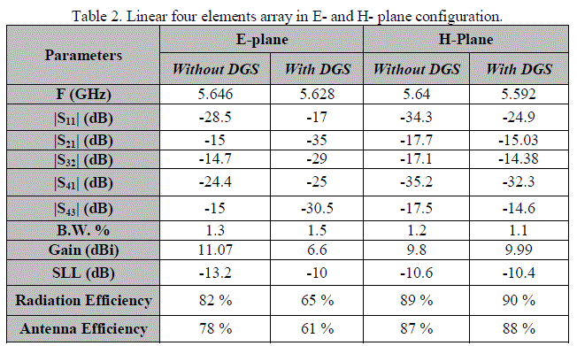
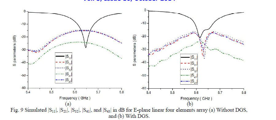
| The simulated |S11|, |S21|, |S32|, |S41|, and |S43| in dB for E-plane linear four elements array without DGS, and with DGS are shown in Fig. 9. From Table 2, it is noticed that DGS antenna resonant frequency is slightly shifts downward with respect to the conventional antenna. |
 |
 |
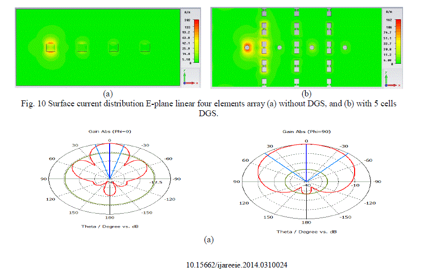
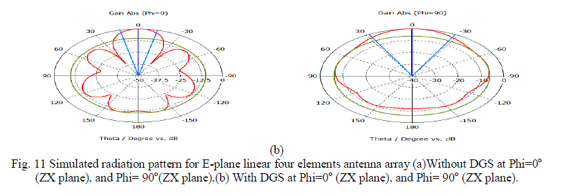
| Fig.10 shows the surface current distribution of the antennaarray in the presence and absence of DGS cells. Clearly, bothof the patches are well coupled at the resonant frequency whichbecomes restricted as the DGS cells are inserted and the couplingeffect is reduced. The center DGS cells blocked the surfacewaves along the E-plane direction and contributed in alleviating themutual coupling between the elements. The conventional antenna array in E-plane shows a very strong coupling of -15dB due to surface waves pronounced in thick, high permittivity substrate.Since the resonant frequency of the antenna falls inside the DGS band gap, surface waves are suppressed and simulations show that mutual coupling drops to -35 dB which is 20 dB lower than the conventional one, but with reduction in gain and efficiency as shown in Fig. 11. On the other hand, conventional antenna array in H-plane have mutual coupling increasing with DGS, but the gain and efficiency are slightly increased |
 |
 |
VI. PLANAR FOUR ELEMENT ARRAYS |
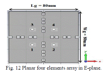
| The four elements microstrip patch antennas array is designed on a dielectric substrate with εr= 10.2, h = 1.27 mm. The distance between the patches is 25 mm (0.47λ0). The defected ground plane is 80 mm x 85 mm (1.5λ0 x 1.6λ0) at resonant frequency. Each patch is TM10 mode excited by a matched coaxial feed 0.7375 mm away from the patch center as shown in Fig. 12. |
 |
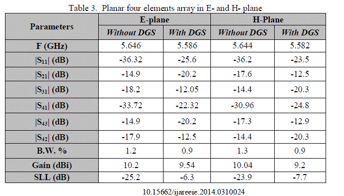
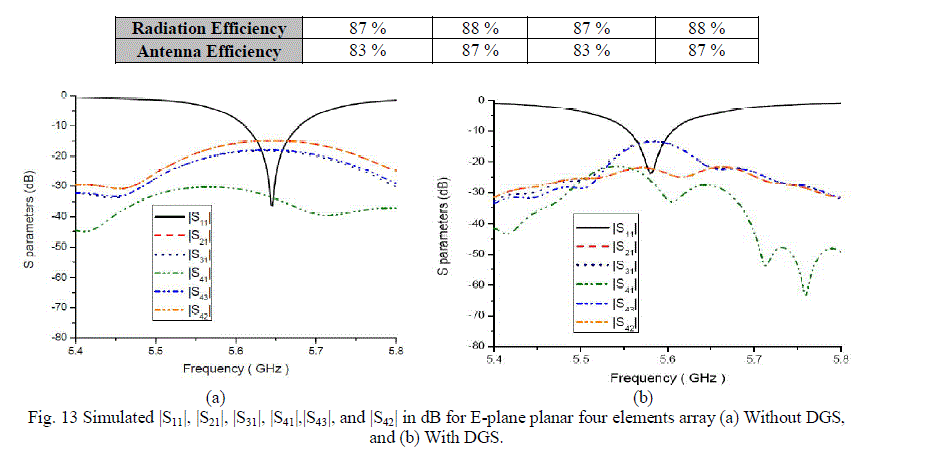
| The simulated |S11|, |S21|, |S31|, |S42|, and |S43| in dB for E-plane linear four elements array without DGS, and with DGS are shown in Fig. 13. As shown in Table 3, it is observed that DGS antenna resonant frequency shifts downward with respect to the conventional antenna. This small frequency shift is due to slow-wave effects of DGS. |
 |
|
 |
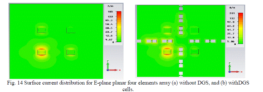
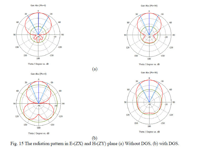
| Fig. 14 shows the surface current distribution of the antenna array with and without DGS cells. Clearly, both of the patches are well coupled at the resonant frequency which becomes restricted as the DGS cells are inserted and the coupling effect is reduced. The conventional antenna array in E-plane shows a very strong coupling of -14.9 dB due to surface waves pronounced in thick, high permittivity substrate. Since the resonant frequency of the antenna falls inside the DGS band gap, surface waves are suppressed and simulations show that mutual coupling drops to -22.08 dB which is 7.18 dB lower than the conventional one, but with slight reduction in gain and small increase in efficiency as shown in Fig. 15. Also, in the H-plane array there is a little reduction in the mutual coupling, slight reduction in gain and small increase in efficiency |
 |
 |
VII. EXPERIMENTAL RESULTS AND DISCUSSION |
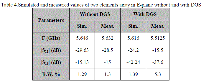
| To verify the conclusions drawn from the simulation, two microstrip antennas were fabricated on Roger RT/Duroid 6010 substrates. The permittivity of the substrate is 10.2, and the substrate thickness is 1.27 mm (50 mil). It is observed that both antennas resonate at 5.646 GHz with return loss better than 10 dB. |
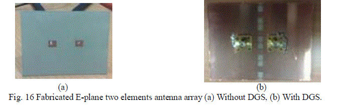 |
| Fig. 16 shows a photograph of the fabricated two elements antennas with and without the DGS. The antenna’s size is 7.375mm x 6 mm, and the distance between the antennas’ center is 25 mm (0.47λ0). The antennas are fabricated on a ground plane of 80 mm x 60 mm (1.5λ0 x 1.2λ0). Comparison between measured values without and with DGS is reported in Table 4. |
 |
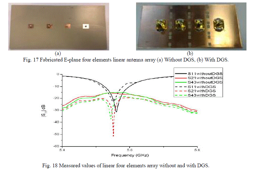
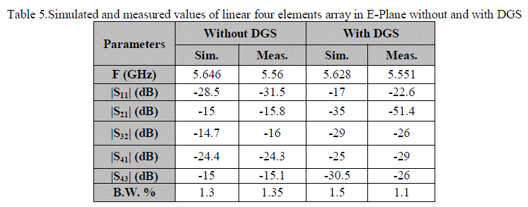
| Linear four elements Array were also fabricated on the previous substrate parameters as shown in Fig. 17. The measured results without and with DGS are compared in Fig. 18. Comparison between measured values without and with DGS is reported in Table 5. |
 |
| For the antennas without the DGS structure, the mutual coupling at 5.86 GHz is -15 dB. In comparison, the mutual coupling of the antennas with the DGS structure is -35 dB. An approximately 20 dB reduction of mutual coupling is achieved at the resonant frequency of 5.646 GHz. This result agrees well with the simulated results. From this experimental demonstration, it can be concluded that the DGS can be utilized to reduce the antenna mutual coupling between array elements |
 |
VIII. CONCLUSION |
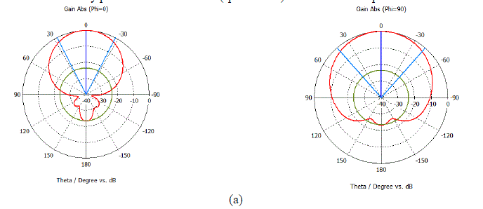
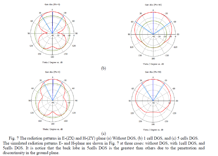
| A low mutual coupling design for two and four elements microstrip antenna array were proposed. A new distribution for dumbbell shaped defect on the ground plane of the antenna is inserted between the patches creating a band gap in the operation frequency band of the antenna. By suppressing the surface waves, it provides a very low mutual coupling between array elements. The DGS antenna was analyzed using a finite integration technique (FIT) and a mutual coupling reduction of 35.6dB was achieved. The analysis indicates that increasing number of dumbbells reduces the mutual coupling between elements. Radiation patterns have minimal change in the broadside direction but back lobe level is increased. However, the gain and the efficiency are decreased due to penetration of DGS in the ground plane. The results agree with those obtained by the waveguide simulator method. |
References |
|